
A. Real Pain Points for Engineers & Procurers
- A 0.15 difference in dielectric constant (Dk) causes 9% impedance deviation in 50Ω high density interconnect traces, failing signal integrity tests.
- Using mismatched CTE materials leads to 27% of microvia failures in automotive hdi circuit boards after 1,000 thermal cycles.
- Overlooking laser drill compatibility for ultra-low-loss materials adds 12–15 days to hdi printed circuit board production lead times.
- Incorrect trace width (below 3mil) for 100Gbps signals increases insertion loss by 40%, violating IEEE 802.3bs standards.
- Material over-specification (e.g., Rogers 4350B for ≤10Gbps designs) raises hdi pcb costs by 55% unnecessarily.
- Poor stackup symmetry results in 0.8mm/m warpage for 16-layer high density interconnect pcb, preventing component placement.
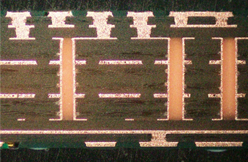
Learn more about :How to Design HDI Microvia PCB
B. Core Technical Points
1. Core Design Principles for 2026
Standard Alignment & Performance Priorities
- Adhere to IPC-2226 (HDI structure design) and IPC-6012 Class 3 (performance specification) for critical applications.
- Prioritize signal integrity for 100Gbps+ data rates with <0.3dB/inch insertion loss at 20GHz.
- Balance miniaturization (trace/space down to 2.5mil/2.5mil) with manufacturability (yield ≥90%).
- Integrate thermal management for 300W/in² power density in AI-focused hdi board designs.
- Ensure compatibility with sequential lamination (up to 4 cycles) for complex buildup structures.
Key Design Trade-Offs
| Priority | Compromise | Quantified Impact |
|---|---|---|
| Ultra-fine traces (2mil) | Reduced current capacity | 0.5oz copper carries 1.2A vs. 1.8A for 3mil traces |
| High layer count (20+) | Increased warpage risk | 0.6mm/m vs. 0.3mm/m for 12-layer designs |
| Stacked microvias (4-level) | Higher manufacturing cost | 30% price premium vs. staggered vias |
2. Material Selection Guidelines
2026 Recommended Materials & Specs
| Material | Dk @10GHz | Df @10GHz | Tg (°C) | Speed Range | HDI Application |
|---|---|---|---|---|---|
| FR408HR | 3.48–3.67 | 0.0093–0.0098 | 180 | 10–25Gbps | Enterprise switches |
| Isola I-Speed | 3.45–3.55 | 0.0059 | 180 | 25–50Gbps | 5G small cells |
| Rogers 4350B | 3.48 | 0.0017 | 180 | ≥25Gbps | RF/microwave modules |
| TU933+ | 3.16 | 0.0021 | 220 | 50–100Gbps | HPC backplanes |
| Astra MT77 | 2.95–3.01 | 0.0017–0.0019 | 200 | 60–100GHz | mmWave AiP |
| Tachyon-100G | 2.98–3.05 | 0.0014–0.0017 | 185 | 100Gbps+ | Optical transceivers |
| Megron 6 | 3.37–3.61 | 0.004 | 180 | 25–50Gbps | PCIe 5.0 servers |
| Megron 7 | 3.2–3.3 | 0.003 | 200 | 60Gbps | Cloud switches |
| Megron 8 | 3.0–3.1 | 0.0025 | 220 | 120Gbps+ | AI accelerators |
Material Selection Decision Framework
- For consumer electronics (≤10Gbps): FR408HR (cost-effective, Dk stability ±0.08)
- For automotive ADAS (25–50Gbps): TU933+ (high Tg, low CTE 14ppm/°C)
- For 5G mmWave (60–100GHz): Astra MT77 (ultra-low Dk, moisture absorption <0.08%)
- For AI/HPC (100Gbps+): Megron 8 + Tachyon-100G (low Df, Dk drift <0.05 up to 40GHz)
- Quality Control: Verify Dk/Df via VNA testing (1GHz/10GHz/20GHz) per IPC-TM-650 2.5.5.12.
3. Stackup & Layer Design
Optimal Stackup Configurations
- 4+N+4 buildup: For 16–20 layer hdi pcb (supports 4-level stacked microvias)
- 2+8+2 structure: Balanced density for 12-layer high density interconnect (AI edge devices)
- 1+N+1: Cost-effective for 6–8 layer consumer hdi circuit boards
- Symmetry Requirement: Mirror layer arrangement (e.g., Signal-GND-Power-Signal) to limit warpage <0.4mm/m.
Layer-Specific Guidelines
- Dielectric thickness: 2–4mil (signal layers), 8–12mil (core layers)
- Reference Planes: 1 ground/power plane per 2 signal layers (minimize loop area <100mm²)
- Copper Weight: 0.5oz (signal layers), 1oz (power planes)
- Compliance: IPC-4104 for dielectric material qualification.
4. Microvia & Via Design
Microvia Specifications
- Diameter: 4–6mil (laser-drilled), aspect ratio ≤0.75:1 (per IPC-6016)
- Stacked Microvias: Up to 4 levels (core-to-buildup transitions)
- Staggered Microvias: Minimum center-to-center distance 0.3mm
- Via-in-Pad: Copper-filled (≥98% fill density) with planarization ≤5μm.
Via Quality Control
- X-ray inspection for buried/stacked vias (wall thickness ≥1mil)
- Microsection analysis (no voids >50μm)
- Thermal cycling (-40°C to 125°C, 1000 cycles) with 0 via failures.
5. Signal Integrity & Impedance Control
Impedance Targets & Tolerances
- Single-ended: 50Ω ±2% (100Gbps+), ±5% (≤25Gbps)
- Differential: 100Ω ±3% (SerDes), 90Ω ±3% (Ethernet)
- Calculation: Account for copper roughness (0.6μm for rolled copper) and dielectric thickness tolerance ±0.1mil.
Signal Routing Best Practices
- Trace length mismatch: ≤3mil for differential pairs
- 45° bends (avoid 90°) to reduce impedance discontinuity
- Guard traces (width ≥3mil) between sensitive high-speed lines
- EMI Mitigation: Ground stitching vias (100mil spacing) around high-frequency traces.
Learn more about: Signal Integrity in HDI PCB Design
6. Trace & Routing Rules
H3: Trace Dimensions by Speed
| Signal Speed | Trace Width (50Ω) | Trace Spacing |
|---|---|---|
| ≤10Gbps | 4mil | 3mil |
| 10–25Gbps | 3.5mil | 3mil |
| 25–50Gbps | 3mil | 2.5mil |
| ≥50Gbps | 2.5mil | 2.5mil |
Routing Constraints
- Maximum trace length: 8 inches for 100Gbps signals (without equalization)
- BGA Fanout: Use via-in-pad for 0.5mm pitch (escape routing ≤2mil trace)
- Power Traces: Minimum width 10mil for 3A current (0.5oz copper)
- Avoid stubs >5mil (cause signal reflections in high-speed paths).
7. Manufacturing & Reliability Requirements
Production Parameters
- Laser Drilling: Ablation rate ≥150 holes/sec (4mil diameter)
- Lamination: Temperature 170–180°C, pressure 350–400psi (sequential cycles)
- Plating: Copper thickness 1mil (via walls), 0.5mil (traces)
- Reflow Compatibility: 260°C peak (10 cycles) for lead-free assembly.
Reliability Testing
- Thermal Cycling: -40°C to 125°C (1000 cycles) – no delamination
- Humidity Testing: 85°C/85%RH (1000hrs) – insulation resistance ≥10¹⁰Ω
- Mechanical Shock: 50g, 11ms pulse (IPC-6012 Class 3)
- Quality Control: AOI + X-ray inspection (100% coverage for microvias).
8. Application-Specific Guidelines
Industry-Specific Requirements
- Automotive (ADAS): ISO 26262 compliance, Tg ≥180°C, CTE ≤16ppm/°C
- 5G Infrastructure: Rogers 4350B + Astra MT77, impedance tolerance ±2%
- AI Servers: 20-layer 4+12+4 stackup, thermal vias (6mil diameter, 100mil spacing)
- Medical Devices: Biocompatible solder mask, IPC-6012 Class 3, 100% visual inspection.
C. Real Factory Case Study
16-Layer HDI for 100Gbps AI Inference Module
Project Specifications
- Stackup: 4+8+4 buildup (16-layer high density interconnect pcb)
- Materials: Megron 8 (signal layers), TU933+ (core), Tachyon-100G (critical paths)
- Parameters: 50Ω/100Ω impedance, 3mil/3mil trace/space, 5mil stacked microvias
- Target: 100Gbps SerDes, 250W power density.
Issues Encountered
- Dk variation (±0.12) in Megron 8 caused 8Ω impedance mismatch (failed eye diagram test)
- Microvia voids (150μm) from inadequate laser drilling power (20W vs. required 25W)
- Warpage (0.7mm/m) due to asymmetric stackup (missing ground plane on layer 15)
- Insertion loss (0.5dB/inch @20GHz) exceeding target (0.35dB/inch).
Implemented Fixes
- Sourced Megron 8 with tight Dk control (3.05±0.03) and pre-qualified via VNA
- Increased laser power to 25W, adjusted drill speed to 100 holes/sec
- Restacked layers (Signal-GND-Power-Signal symmetry), added ground plane on layer 15
- Switched to rolled copper (0.6μm roughness) for signal layers
- Added thermal vias (6mil diameter, 80mil spacing) under hot components.
Results
- Impedance: 50.2±1.1Ω, 100.3±2.2Ω (meets ±2%/±3% targets)
- Insertion loss: 0.32dB/inch @20GHz (36% improvement)
- Warpage: 0.35mm/m (within assembly limits)
- Yield: 94% (up from 72%)
- Thermal Performance: Hotspot temperature reduced from 128°C to 89°C.
D. Common Design Errors (Production Perspective)
- Using through-hole vias in high-density areas: Blocks 3x more routing space than microvias.
- Ignoring Dk frequency dependence: Assuming 10GHz Dk applies to 25GHz signals causes impedance drift.
- Inadequate via fill: Voids >50μm lead to 40% higher thermal resistance.
- Overlooking prepreg drying: Moisture >0.15% results in delamination during reflow.
- Trace width inconsistency: ±0.5mil variation causes 7% impedance deviation.
- Insufficient ground stitching: Spacing >150mil increases EMI by 18dB.
E. FAQ
- What is the difference between HDI PCB and standard PCB in design? HDI PCB uses microvias (4–6mil), finer trace/space (2.5–3mil), and buildup layers, while standard PCB relies on through-hole vias (≥8mil) and 3–4mil trace/space. HDI supports higher density (20+ pads/cm² vs. 10 pads/cm²) and faster signals (100Gbps+ vs. ≤10Gbps).
- How to select between stacked and staggered microvias for HDI? Choose stacked microvias for maximum density (AI/HPC), but ensure manufacturer capability for 4-level stacking. Staggered microvias are more cost-effective and reliable for automotive/industrial hdi circuit boards (lower alignment risk).
- Which materials are best for 100Gbps+ HDI PCB designs? Megron 8 (low Df=0.0025), Tachyon-100G (Dk=2.98–3.05), and TU933+ (high thermal stability) are optimal. Combine with rolled copper (Ra≤0.8μm) to minimize conductor loss.
- How to avoid warpage in multi-layer HDI PCB? Use symmetric stackup, maintain uniform copper distribution (±10% across layers), select low-CTE materials (X/Y CTE 12–16ppm/°C), and control lamination temperature ramp rate (2°C/min).
If you need professional HDI PCB design support or quotation, our team provides free DFM check and fast turnaround.


![Understanding PCB Costs & Pricing [Your Complete Guide]](https://hdicircuitboard.com/wp-content/uploads/elementor/thumbs/Understanding-PCB-Costs-Pricing-Your-Complete-Guide-qzzhe6mcaxuolkux3xalfktgavumi9y1aqfbs9bpv4.webp "Understanding PCB Costs & Pricing [Your Complete Guide]")


