
Engineering Challenges in HDI Impedance Control
High density interconnect PCBs rely on tightly controlled impedance to support high-speed signals, yet inconsistent implementation creates costly production and performance risks. Even small deviations from 50Ω, 75Ω, or 100Ω targets lead to signal reflection, crosstalk, compliance failures, and reduced manufacturing yield. Miniaturized HDI features—including fine traces, thin dielectrics, and laser-drilled microvias—amplify sensitivity to material, layout, and process variations, requiring precision engineering at every stage from stack-up design to final testing.
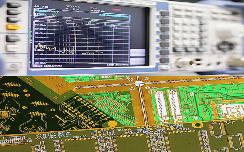
Learn more about: How to Calculate Impedance for HDI Boards
50Ω Impedance in HDI PCBs
Primary Applications
50Ω impedance is the industry standard for single-ended high-speed and RF signal paths in HDI printed circuit boards.
- DDR5, LPDDR5, and high-speed memory interfaces
- PCIe 5.0, PCIe 6.0, and SerDes channels
- 2.4GHz / 5GHz / 6GHz Wi-Fi, Bluetooth, and sub‑6GHz 5G RF paths
- General clock signals and high-speed I/O
HDI-Specific Design Parameters
- Microstrip (outer layers): 3.5–5mil trace width on 4mil dielectric
- Stripline (inner layers): 4–5.5mil trace width between 4mil dielectric layers
- Microvias: 6–8mil laser‑drilled, 1.5x anti‑pad diameter, staggered layout
- Solder mask compensation: –2Ω to –3Ω adjustment for 0.5–1mil thickness
Standards & Tolerances
- IPC‑2221: ±10% for Class 2, ±5% for Class 3 high‑speed HDI
- PCI‑SIG: ±5% for PCIe 5.0/6.0
- JEDEC: ±7% for DDR5 memory signaling
- Test method: IPC‑TM‑650 2.5.5.12 TDR measurement
75Ω Impedance in HDI PCBs
Primary Applications
75Ω impedance supports video, broadcast, and RF systems in compact HDI board designs.
- HDMI 2.1, SDI, and professional video interfaces
- RF coaxial pathways, cable TV, and satellite communication
- 5G small‑cell front‑end modules
- Medical imaging and long‑reach sensor links
HDI-Specific Design Parameters
- Microstrip: 6–8mil trace width on 4mil dielectric
- Stripline: 7–9mil trace width for embedded layers
- Minimum keep‑out zone: 30mil from adjacent signal traces
- Trace curvature radius: ≥10x trace width to preserve impedance stability
Standards & Tolerances
- SMPTE ST 292: ±10% for 3G‑SDI video
- HDMI Forum: ±15% for TMDS differential signaling
- IPC‑6012: ±10% for all reliability classes
- Return loss requirement: ≥15dB at operating frequency
100Ω Impedance in HDI PCBs
Primary Applications
100Ω differential impedance enables noise‑immune, high‑bandwidth data transmission in HDI PCBs.
- 10G / 25G / 100G Ethernet differential pairs
- USB4, Thunderbolt 3/4, and high‑speed serial links
- LVDS, SATA III, and SAS‑4 data buses
- Automotive ADAS, infotainment, and industrial communication
HDI-Specific Design Parameters
- Microstrip differential pair: 4–5mil width, 5–7mil spacing
- Stripline differential pair: 4.5–6mil width, 6–8mil spacing
- Length matching tolerance: ±2mil across the pair
- Maximum 2 vias per differential pair; symmetric placement required
Standards & Tolerances
- IEEE 802.3: ±10% for Ethernet physical layers
- USB‑IF: ±10% for USB4 and Thunderbolt
- IPC‑2221: ±5% for Class 3 high‑speed HDI
- Skew limit: <5mil for 25Gbps+ signals
50Ω / 75Ω / 100Ω Impedance Full Comparison Table
| Impedance Type | Primary Applications | HDI Design Parameters | Standards & Tolerances | Material Requirements | Manufacturing Controls | Testing & Validation |
|---|---|---|---|---|---|---|
| 50Ω Single-Ended | DDR5, PCIe, RF, Clock | Microstrip: 3.5–5mil Stripline: 4–5.5mil Dielectric: 2–4mil Microvia: 6–8mil |
IPC-2221 ±5%~±10% PCI-SIG ±5% JEDEC ±7% |
FR4 Dk=3.6–3.8 Df ≤0.008 Cu Ra ≤1μm |
Etch factor 1.5–2.0 Dielectric ±0.1mil Solder mask compensation |
TDR IPC-TM-650 VNA 1–40GHz Microsection |
| 75Ω Single-Ended | HDMI, SDI, Video, RF | Microstrip: 6–8mil Stripline: 7–9mil Keep-out: 30mil Symmetric routing |
SMPTE ±10% HDMI Forum ±15% IPC-6012 ±10% |
Low-Dk 3.0–3.4 High-Tg ≥180°C Low loss |
No plane gaps Cu roughness control Uniform lamination |
Return loss ≥15dB Insertion loss ≤0.5dB/in TDR / VNA |
| 100Ω Differential | Ethernet, USB4, LVDS, ADAS | W:4–5mil, S:5–7mil Stripline preferred Length match ±2mil Symmetric vias |
IEEE 802.3 ±10% USB-IF ±10% IPC-2221 ±5%~±10% |
High-speed FR4 Dk=3.4–3.6 Df ≤0.005 |
Spacing ±0.1mil Backdrill stubs <5mil No obstacles between pairs |
Differential TDR Skew measurement Eye diagram |
Microstrip vs. Stripline Comparison for HDI Impedance
| Structure | Impedance Range | HDI Suitability | Solder Mask Impact | Stability |
|---|---|---|---|---|
| Microstrip | 50Ω / 75Ω | Outer layers, simplified routing | –2Ω to –3Ω | Medium |
| Stripline | 50Ω / 100Ω | Inner high-speed layers | Negligible | High |
HDI-Specific Considerations for All Impedance Values
Material Selection
- Standard FR4: Dk 3.8–4.2 for general 50Ω / 100Ω HDI
- High‑speed FR4: Dk 3.4–3.6, Df ≤0.008 for 25Gbps+ signals
- Low‑Dk laminates: Dk 3.0–3.2 for 75Ω RF and video paths
- Smooth copper: Ra ≤0.8μm for reduced insertion loss above 10GHz
Manufacturing Controls
- Dielectric thickness tolerance: ±0.1mil
- Trace etching uniformity: ±0.2mil across the panel
- Laser drill accuracy: ±1mil for microvias
- Lamination pressure: 300–400 psi for consistent dielectric properties
Testing & Validation
- 100% TDR testing for Class 3 HDI printed circuit boards
- Impedance test coupons matching production stack‑up
- VNA verification for insertion loss and return loss
- Microsection analysis for dielectric and trace geometry
HDI Board Factory Case Study
12-Layer HDI for 25Gbps Ethernet & HDMI 2.1
- Layer structure: 12‑layer high density interconnect PCB, 2+8+2 buildup
- Impedance targets: 50Ω, 75Ω, 100Ω
- Initial issues: 50Ω at 45Ω, 75Ω high insertion loss, 100Ω pair mismatch
- Corrections: trace width adjustment, low‑roughness copper, symmetric routing, lamination optimization
- Final results: impedance within ±0.5% of target, yield improved from 72% to 94%, full compliance achieved
Common Design Errors from Production View
- Ignoring microvia inductance (0.1nH per via) causing 1–2Ω spikes
- Using generic Dk=4.0 instead of frequency‑corrected values
- Unequal differential spacing creating 5–7Ω mismatch
- Uncompensated solder mask reducing microstrip impedance by 2–3Ω
- Reference plane gaps increasing impedance by 10–15%
- Test coupons not matching HDI stack‑up, leading to invalid measurements
Learn more about : HDI PCB Impedance Control: Design, Manufacturing & Performance Guide
FAQ
- What is the primary purpose of 50Ω, 75Ω, and 100Ω impedance in HDI PCBs? 50Ω supports digital and RF performance, 75Ω optimizes video and RF loss, and 100Ω enables noise‑immune differential signaling in high density interconnect designs.
- How do microvias influence impedance in HDI boards? Each microvia introduces small parasitic inductance that creates local impedance discontinuities. Staggered vias, stitching vias, and trace width compensation restore stability.
- Why is stripline preferred for 100Ω differential HDI signals? Stripline provides shielding, consistent dielectric environment, and minimal crosstalk, which supports stable impedance and signal integrity at high data rates.
- What testing methods validate impedance in HDI production? TDR measures impedance values per IPC standards, while VNA verifies insertion and return loss. Microsectioning confirms physical trace and dielectric dimensions.
If you need HDI PCB with impedance control,contact our engineering team for a free DFM check.


![Understanding PCB Costs & Pricing [Your Complete Guide]](https://hdicircuitboard.com/wp-content/uploads/elementor/thumbs/Understanding-PCB-Costs-Pricing-Your-Complete-Guide-qzzhe6mcaxuolkux3xalfktgavumi9y1aqfbs9bpv4.webp "Understanding PCB Costs & Pricing [Your Complete Guide]")


