- Blind vias, buried vias, Ultra HDI PCB
- High frequency low loss PCB material
- TLY-5, RF35, RF-35TC, TSM-DS3, TLX-8, TLX-9 material
- RO4003, RO4350B, RO4835, RT/duroid 5870, RT/duroid 5880, RT/duroid 6002, TMM3, TMM4, TMM6, TMM10, TMM10i material
RF PCB Solutions | Custom Design & Microwave Circuit Board Manufacturing
RF PCB Basics & Material Selection
What is RF PCB
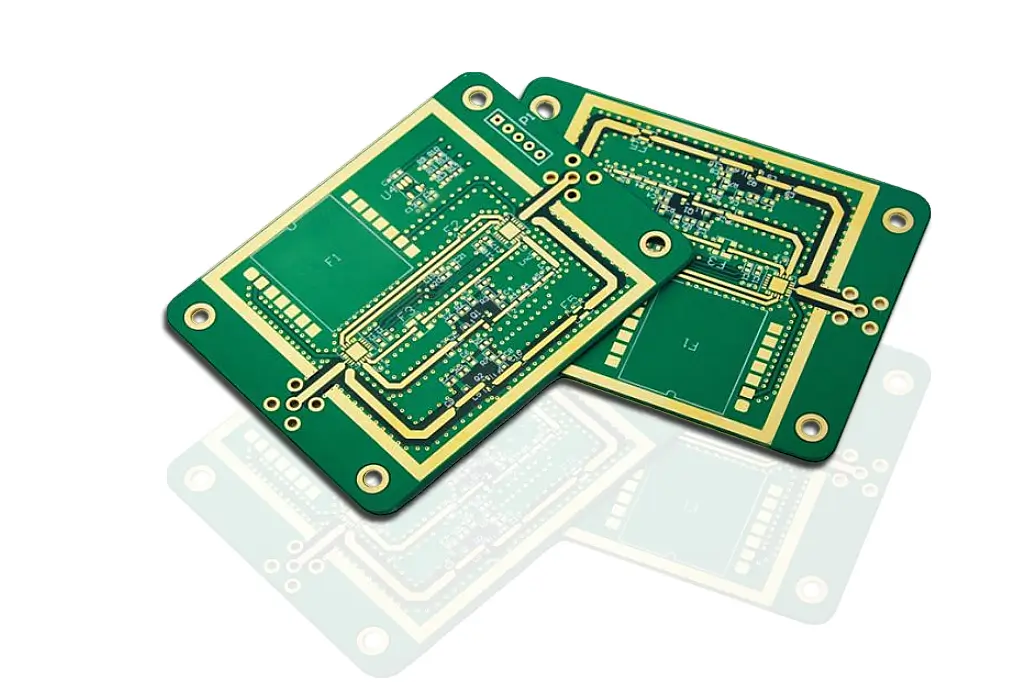
An RF PCB—also known as an RF circuit board or microwave circuit board—is a specialized printed circuit board engineered exclusively for radio frequency (3kHz–300GHz) and microwave (1GHz–300GHz) signal transmission. Its core performance attributes include ultra-low dielectric loss (Df≤0.004) and a stable dielectric constant (Dk) across broad frequency bands, a combination that standard high-frequency PCBs cannot replicate. Unlike conventional high-frequency boards, RF PCBs minimize signal reflection and electromagnetic interference (EMI), making them a critical component for 5G microwave backhaul systems, 77GHz automotive radar, and military communication equipment. All our RF PCB products adhere strictly to IPC-6012 and IPC-2226 RF-specific standards, with impedance control tolerance locked at ±5% to meet the stringent demands of microwave-grade applications.
RF PCB Core Material & Custom Shielding Solutions
We offer a proprietary portfolio of three RF PCB material categories paired with custom RF shielding PCB solutions, tailored to distinct microwave frequency bands and anti-interference requirements— a offering that sets us apart from generic PCB suppliers:
- PTFE-Based Substrates (Rogers RO4350B/5880): Boasting a Dk range of 3.48–3.55 and Df range of 0.0009–0.0037, these substrates are optimized for 24–77GHz automotive radar and satellite microwave circuit board projects. They deliver exceptional thermal stability (-55°C to 125°C), ensuring consistent performance in extreme operating environments.
- Ceramic-Filled Laminates (Isola Astra MT77): With a Dk of 3.0 and Df of 0.0017, this material is ideal for 6–24GHz 5G microwave backhaul RF PCBs. It strikes a precise balance between high-frequency performance and cost efficiency, making it suitable for large-scale mass production.
- FR-4 Hybrid Materials: Featuring a Dk of 3.8 and Df of 0.008, this is a cost-effective alternative for 3–6GHz industrial RF devices. When paired with our copper-clad RF shielding PCB technology, it reduces EMI by 40% compared to unshielded boards, meeting the anti-interference needs of mid-range RF applications.
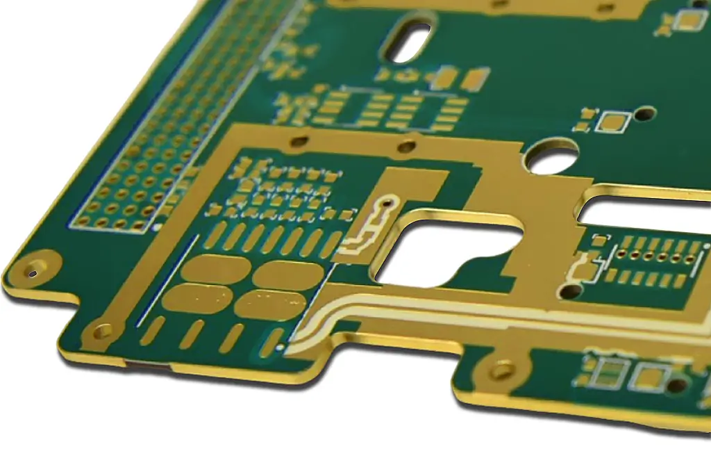
RF PCB Custom Design & Stackup Services
RF PCB Design Guidelines & Precision Impedance Control
Our RF PCB design service follows five microwave-exclusive guidelines to guarantee signal integrity—standards that far exceed basic high-frequency design rules:
- Dynamic Impedance Calibration: Design 50Ω (RF) or 75Ω (microwave) characteristic impedance with a ±2% tolerance. For 77GHz radar RF circuit boards, we use advanced 3D electromagnetic simulation to eliminate impedance mismatch, a common flaw in traditional design workflows.
- Curved Trace Routing Optimization: Use curved traces with a bend radius of ≥3x the trace width for RF PCBs to minimize signal reflection. Maintain a spacing of 2x the trace width between RF and digital traces to completely avoid cross-signal interference.
- Shielded Ground Plane Engineering: Add a continuous ground plane with 0.1mm via stitching (spaced ≤λ/20, where λ equals microwave wavelength) for RF shielding PCBs, creating a 360° EMI shield that protects sensitive microwave signals from external interference.
- Strategic Component Placement: Position RF transceivers and antennas within 5mm of each other to shorten signal paths and reduce attenuation. Place 0402-size decoupling capacitors ≤0.3mm from chip pins to suppress noise and stabilize power supply for high-frequency components.
- Microvia Optimization for Microwave Signals: Use blind/buried vias with a diameter of ≤0.1mm to eliminate stub length (≤0.3mm), a modification that drastically reduces signal reflection in microwave circuit board designs.
Hybrid RF PCB Stackup Optimization Services
Our hybrid RF PCB stackup optimization service addresses the core pain point of material compatibility for mixed-signal RF projects— where RF and digital circuits coexist on a single board:
- Layer Segmentation for Mixed-Signal Performance: Design a 4-layer hybrid stackup (RF top layer → ground plane → power plane → digital bottom layer) for 5G microwave backhaul RF PCBs. We use Rogers RO4350B for the RF layer to ensure high-frequency performance, paired with high-Tg FR-4 for digital layers to optimize cost efficiency.
- CTE Matching to Prevent Delamination: Match the coefficient of thermal expansion (CTE) of RF and FR-4 layers to a difference of ≤10ppm/°C, avoiding delamination during high-temperature lamination. This solves a common failure mode in unoptimized hybrid microwave circuit boards.
- No-Flow Prepreg for Stackup Precision: Use no-flow prepreg for hybrid RF PCBs to maintain stackup thickness tolerance of ±5μm, ensuring consistent impedance across the entire board surface— a critical factor for microwave signal stability.
All stackup designs include a detailed electromagnetic simulation report to validate microwave signal performance before prototyping, eliminating costly design iterations.
RF PCB Manufacturing & Testing Processes
RF PCB Precision Fabrication Techniques
Our RF PCB manufacturing process incorporates four RF-exclusive techniques— a core differentiator that sets us apart from standard high-frequency PCB production lines:
- UV Laser Drilling for Microvias: Use UV laser drilling with 3μm precision to create 0.1mm blind vias in RF PCBs. This avoids mechanical drill vibration, which can cause via voids, and achieves a void rate of ≤0.3% in critical microwave signal paths.
- Micron-Level Lamination Control: Maintain prepreg thickness tolerance of ±3μm during microwave circuit board lamination. At 77GHz, even a 1μm thickness variation can cause a 0.5Ω impedance deviation— a margin that is unacceptable for high-precision RF applications.
- Selective Plating for Cost-Performance Balance: Apply gold plating of ≥0.05μm to RF signal pads of RF PCBs to improve solderability and reduce oxidation, while using electroless nickel immersion gold (ENIG) for digital layers to cut production costs without compromising functionality.
- Chemical Planarization for Via-in-Pad: Perform chemical planarization on filled vias for RF shielding PCBs, ensuring surface flatness of ≤10μm. This enables reliable assembly of fine-pitch BGA components with a 0.2mm pitch, a requirement for compact RF modules.
RF PCB Microwave Performance Testing Protocols
As a specialized RF PCB manufacturer, our quality control system includes six microwave-exclusive tests— far exceeding the scope of standard PCB inspections:
- Vector Network Analyzer Testing: Measure insertion loss (≤0.4dB/inch at 24GHz) and return loss (≥15dB at 77GHz) for each RF PCB panel, validating microwave signal integrity across the entire frequency range.
- Phase Stability Validation: Confirm phase shift ≤3° at 77GHz for automotive radar microwave circuit boards, ensuring accurate target detection and tracking— a key requirement for advanced driver-assistance systems (ADAS).
- ESD Shielding Efficacy Testing: Verify RF shielding PCB performance (≥60dB EMI attenuation at 24GHz) for military communication projects, fully complying with MIL-STD-461E electromagnetic compatibility standards.
- High-Resolution X-Ray Inspection: Check blind/buried vias for voids and plating defects, enforcing a maximum void rate of ≤0.3% to eliminate signal reflection points in microwave paths.
- Aerospace-Grade Thermal Cycling: Subject aerospace-grade RF PCBs to 1000 cycles of -55°C to 125°C, simulating years of extreme temperature stress to validate long-term reliability.
- Post-Assembly Impedance Retest: Conduct 100% impedance testing after component assembly to ensure that soldering processes do not cause performance degradation in RF signal paths.
All product batches are accompanied by a comprehensive test report, suitable for regulatory submissions such as FCC certification for telecom devices and MIL-STD compliance for military applications.
RF PCB Industry Application Cases
Automotive 77GHz Radar RF PCB Case Study
We delivered over 300,000 RF PCB units to a leading automotive OEM, leveraging Rogers RO5880 material and our specialized RF PCB design service to achieve ±2% impedance control and ≤0.4dB/inch insertion loss at 77GHz. The microwave circuit board integrated our copper-clad RF shielding PCB technology to reduce EMI interference from the vehicle’s powertrain, achieving a 99.9% first-pass yield in mass production. The resulting radar module achieved a 150m detection range— 10% longer than competitor boards— helping the OEM meet NCAP 5-star safety standards for collision avoidance systems.
5G Microwave Backhaul RF PCB Case Study
Our RF PCBs were deployed in 5G microwave backhaul base stations for a global telecom vendor, using Isola Astra MT77 material and our hybrid stackup design to support 24GHz signal transmission. The RF circuit board reduced signal latency by 20% compared to traditional FR-4 boards and passed FCC Part 15 certification, enabling the vendor to expand 5G coverage in rural areas where fiber optic infrastructure is unavailable.
RF Microwave PCB Capabilities
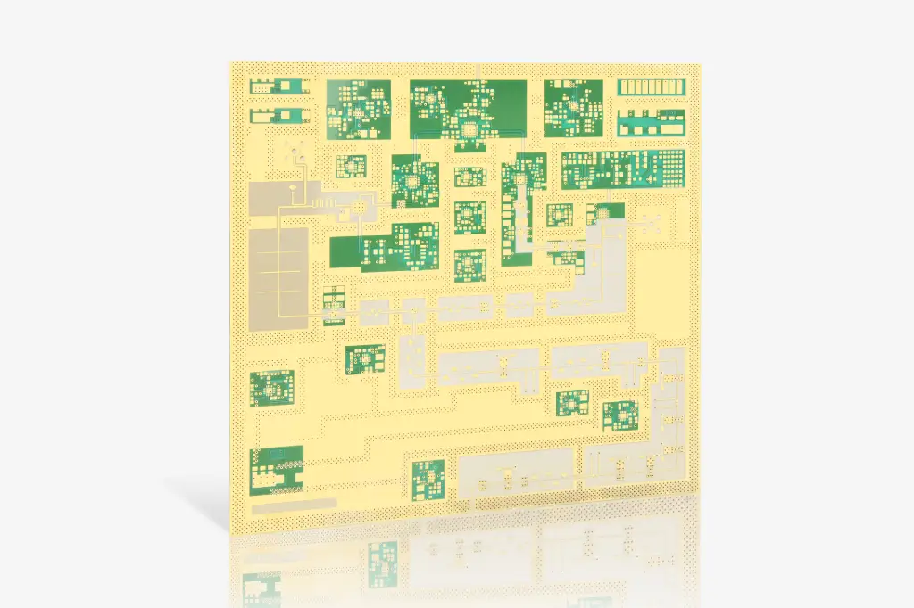
We pride ourselves on having the deep engineering experience and advanced technology and equipment to handle any project all the way from layout through assembly in our state-of-the-art facility. This includes fabrication and manufacturing of radio frequency (RF) and microwave PCBs.
RF PCB Design Guidelines
Download our design guidelines for RF PCBs
To prevent getting it wrong from the start, we have put together our design guidelines, to use as a checklist.
The file lists some of the fabrication features that are typically associated with RF PCB. The feature limits listed are not comprehensive; Our experienced engineers have also worked with every type of PCB material, so they have the knowledge and expertise to provide recommendations and answer all of your RF PCB questions. Most importantly, they know how to assist for manufacturability and the potential cost drivers of a project.
| Description | Production | Advanced |
|---|---|---|
| Inner Layer | ||
| Min.Trace/Space | 1.5mils / 1.5mils | 1.2mils / 1.5mils |
| Min. Copper Thickness | 1/3oz | 1/7 oz |
| Max. Copper Thickness | 10oz | 30oz |
| Min. Core Thickness | 2mils | 1.5mils |
| Line/ pad to drill hole | 7mils | 6mils |
| Line/ pad to board edge | 8mils | 7mils |
| Line Tolerance | +/-10% | +/-10% |
| Board Dimensions | ||
| Max. Finish Board Size | 19”X26” | 20”X28” |
| min. Finish Board Size | 0.2"X0.2" | 0.15"X0.15" |
| Max. Board Thickness | 0.300"(+/-10%) | 0.350"(+/-8%) |
| Min. Board Thickness | 0.007"(+/-10%) | 0.005"(+/-10%) |
| Lamination | ||
| Layer Count | 60L | 100L |
| Layer to Layer Registration | +/-4mils | +/-2mils |
| Drilling | ||
| Min. Drill Size | 6mils | 5mils |
| Min. Hole to Hole Pitch | 16mils(0.4mm) | 14mils(0.35mm) |
| True position Tolerance | +/-3mils | +/-2mils |
| Slot Diameter Tolerance | +/-3mils | +/-2mils |
| Min gap from PTH to track inner layers | 7mils | 6mils |
| Min. PTH edge to PTH edge space | 9mils | 8mils |
| Plating | ||
| Max. Aspect Ratio | 28:1 | 30:1 |
| Cu Thickness in Through hole | 0.8-1.5 mils | 2 oz |
| Plated hole size tolerance | +/-2mils | +/-1.5mils |
| NPTH hole tolerance | +/-2mils | +/-1mils |
| Min. Via in pad Fill hole size | 6mils | 4mils |
| Via in pad Fill Material | Epoxy resin/Copper paste | Epoxy resin/Copper paste |
| Outer Layer | ||
| Min. Trace/Space | 2mils / 2mils | 1.5mils / 1.5mils |
| Min. pad over drill size | 6mils | 5mils |
| Max. Copper thickness | 12 oz | 30 oz |
| Line/ pad to board edge | 8mils | 7mils |
| Line Tolerance | +/-15% | +/-10% |
| Metal Finish | ||
| HASL | 50-1000u” | 50-1000u” |
| HASL+Selective Hard gold | Yes | Yes |
| OSP | 8-20u” | 8-20u” |
| Selective ENIG+OSP | Yes | Yes |
| ENIG(Nickel/Gold) | 80-200u”/2-9 u” | 250u”/ 10u” |
| Immersion Silver | 6-18u” | 6-18u” |
| Hard Gold for Tab | 10-80u” | 10-80u” |
| Immersion Tin | 30u”min. | 30u” min. |
| ENEPIG (Ni/Pd/Au) | 125u"/4u"/1u” min. | 150u"/8u"/2u” min. |
| Soft Gold (Nickel/ Gold) | 200u”/ 20u”min. | 200u”/ 20u” |
| Solder Mask | ||
| S/M Thickness | 0.4mils min. | 2mils max. |
| Solder dam width | 4mils | 3mils |
| S/M registration tolerance | +/-2mils | +/-1.5mils |
| S/M over line | 3.5mils | 2mils / 2mils |
| Legend | ||
| Min. Space to SMD pad | 6mils | 5mils |
| Min. Stroke Width | 6mils | 5mils |
| Min. Space to Copper pad | 6mils | 5mils |
| Standard Color | White , Yellow, Black | N/A |
| Electrical Testing | ||
| Max. Test Points | 30000 Points | 30000 Points |
| Smallest SMT Pitch | 16mils(0.4mm) | 12mils(0.3mm) |
| Smallest BGA Pitch | 10mils(0.25mm) | 6mils(0.15mm) |
| NC Rout | ||
| Min. Rout to copper space | 8mils | 7mils |
| Rout tolerance | +/-4mils | +/-3mils |
| Scoring (V-cut) | ||
| Conductor to center line | 15mils | 15mils |
| X&Y Position Tolerance | +/-4mils | +/-3mils |
| Score Anger | 30o/45o | 30o/45o |
| Score Web | 10mils min. | 8mils min. |
| Beveling | ||
| bevel anger | 20-71o | 20-71o |
| Bevel Dimensional Tolerance | +/-10mils | +/-10mils |
| Impedance controll | ||
| Impedance controll | +/-10% | +/-7% |
View More +
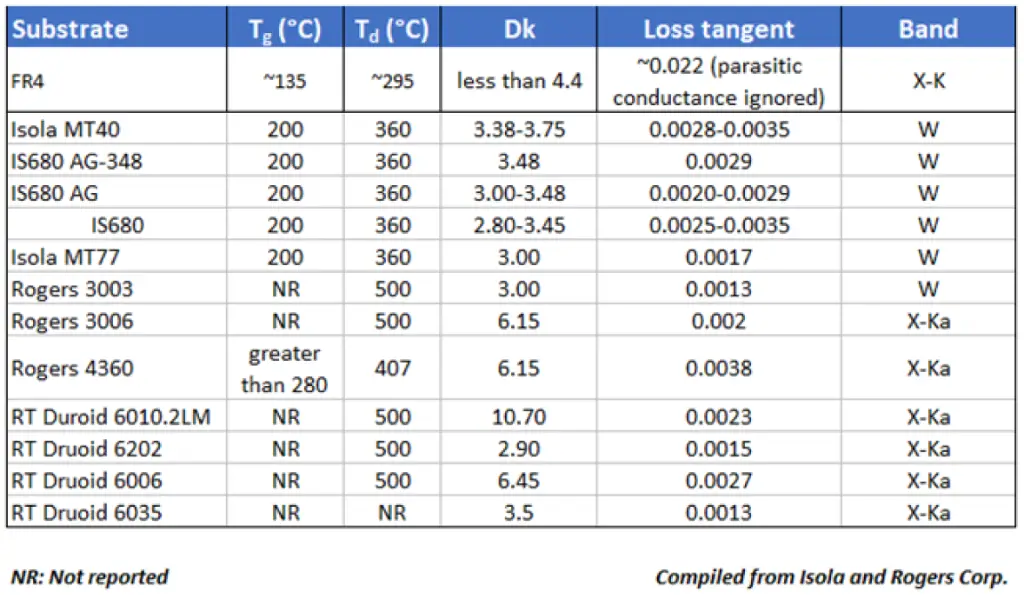
Some dielectric and thermal properties for RF PCB materials.
RF PCB Materials
FR4 materials are acceptable for RF transmission lines and interconnects operating up to WiFi frequencies (~6 GHz). Beyond these frequencies, RF engineers recommend using alternative materials to support RF signal propagation and printed RF circuit designs. Standard FR4 laminates use resin-filled fiberglass weaves to hold components, but these fiber weave effects in certain materials could create signal and power integrity problems if fabrication procedures are not specified properly.
Alternative material systems use PTFE-based laminates and bondply materials to bond a PTFE layer with the next layer in your PCB stackup. These materials have lower loss tangent than FR4 materials, so signals can travel farther without attenuating and still fall within acceptable margins. These laminates should form the substrate that supports RF transmission lines at very high frequencies, such as 77 GHz radar, or for very long interconnects at lower frequencies, such as 6 GHz WiFi. The table below summarizes some important material properties for common RF PCB materials.
This is not a complete list of RF circuit board materials, although the above materials are very popular.
RF Microwave PCB Material Properties
RF microwave PCBs are typically built using advanced composites with very specific characteristics for dielectric constant (Er), loss tangent, and co-efficient of thermal expansion (CTE).
High frequency circuit materials with a low stable Er and loss tangent allow for high speed signals to travel through the PCB with less impedance than standard FR-4 PCB materials. These materials can be mixed in the same stack-up for optimal performance and economics.
Remain extremely stable in high temperature environments while operating at very low to very high frequencies
Allow for the effective placement of very fine pitch components, including in some cases bare die-attach
Facilitate the alignment of multiple layers and the features they represent in a complex PCB layout
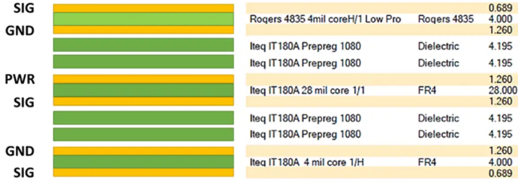
Example hybrid stackup with a Rogers PTFE laminate.
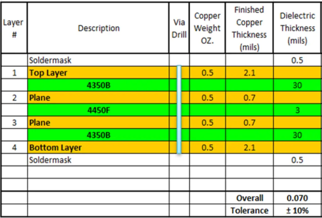
nverted 4-layer stackup using only PTFE materials.
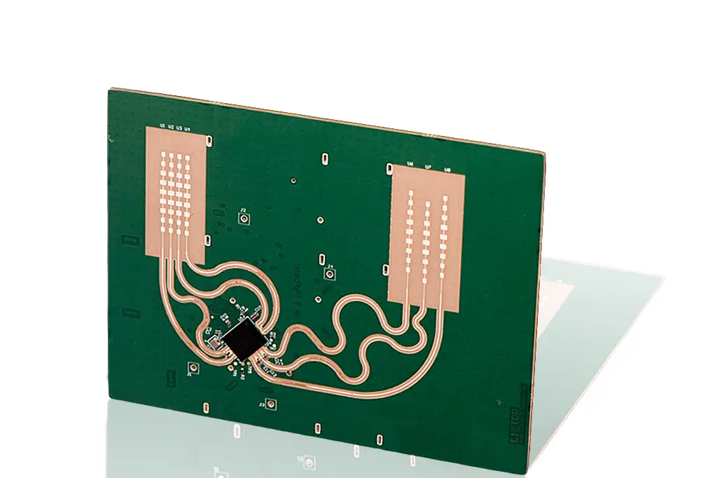
RF Microwave PCB Stackup
Once you’ve selected your laminate and bondply materials for your RF design, it’s time to add them to your stackup. While you could build an entire multilayer PCB stackup with RF materials, it’s generally not needed and can be overly expensive. One option is to build a hybrid stackup, where the RF laminate is placed on a top layer to support RF transmission lines and circuits, and the internal layer is used to support ground planes, routing for digital signals, and power. The opposite layer can also support digital components that need to interface with your RF front end, any ADCs for collecting RF signals, or other components.
If you don’t need a digital section in your RF PCB layout, you can go with a 2-layer or 3-layer PCB with RF laminates that have standard or near-standard thickness. Once you’ve determined the PCB layer thickness and material system, you’ll need to determine the impedance of your RF traces.
Another example without the hybrid material set shown above is given in the stackup table below. In this example, thicker Rogers core materials (RO4350B) are used on the outer layers to provide a thick basis for routing signals on the surface layer with GND on an inner layer. The internal layer is a bondply (RO4450F), and it is used to function as the prepreg that bonds the two cores together. This is just one of many stackup styles used in RF designs. The important point here is the use of bondply layers, which function essentially like prepregs in a standard PCB stackup.
Why would we use a stackup with thicker layers to support circuit designs? There are important reasons for doing this that relate to sizing traces to hit impedance targets while also reducing losses, as well as controlling parasitic capacitance/inductance for components in RF printed circuits.
Hybrid RF Microwave PCB
A hybrid printed circuit board (PCB) multilayer is a PCB that uses dissimilar materials with the intent of optimizing electrical performance and improving system reliability focused towards high-frequency RF applications. The biggest challenge when manufacturing this type of PCB is managing the different coefficient of thermal expansion (CTE) properties of the dissimilar circuit materials both during PCB fabrication and component assembly.
Typically these designs include a combination of FR-4 material and PTFE laminates which allows a designer to condense both RF functionality and RF functionality on the same PCB which can reduce both the footprint of the device and the costs.
All of the world class laminate manufacturers like Isola, Rogers, Arlon, and Taconic all have published significant technical information on the properties and performance of their laminates. In the following sections we will point out some of the capabilities that we provide and some of the items to avoid when designing a RF Hybrid PCB circuit.
Hybrid RF PCB Laminate Construction Considering
When producing a printed circuit board with dissimilar materials it is critically important to have experience in both the physical properties of the laminate and the capabilities of your equipment. Based upon the CTE values of all of the layers of material (ex FR4, PTFE, and Copper) each material grows at a different rate during elevated thermal exposure (i.e. lamination). This can cause significant registration issues as one material shrinks while another one expands and it can also cause delamination of the copper-to-substrate interfaces. Therefore, not all materials should be used in hybrid applications as they are not manufacturable regardless of the desired performance.
Working with your PCB fabricator early in the design process will give you the best results as they are most aware of what materials can work best together. For example, Rogers 5880 is a fantastic RF material used in high reliability applications. The biggest challenge with the material is that it contracts (shrinks) after you etch the copper off so a fabricator needs to understand how that works in their process to compensate for this issue.
Hybrid constructions typically involve a low loss material such as Nelco or Rogers combined with another core material like FR-4.
Hybrid Microwave PCB Stack Up Challenges
A major part of any RF/microwave application is the ability to stay within the specific tolerances of a design so that the required frequencies can be achieved. One of the most difficult challenges in managing the stack-up of a hybrid design is consistently achieving an overall thickness requirement from panel to panel and even piece to piece in some applications. Since there is more than one material type, there will also be more than one prepreg (adhesive system) type that can be used to laminate the design together.
A lot of RF designs have RF signal layers that have large open (un copper filled) areas after etching, a fabricator will use different techniques to assure that there is plenty of insulation between the layers and that we have a consistent overall thickness.
In many instances a no-flow FR-4 prepreg will be the best solution to keep the thickness uniform but that can add material to the overall stack up and change the electrical properties of the entire package.
RF PCB Material Stock
Will all the different features of every RF PCB application, we have developed partnerships with the key material suppliers such as Rogers, Arlon, Nelco, and Taconic just to name a few. While many of the materials are very specialized, we do hold significant stock of product in our warehouse from Rogers (4003 & 4350 series) and Arlon. Not many companies are prepared to do that given the high cost of carrying inventory to be able to respond quickly.
High technology circuit boards fabricated with high frequency laminates can be difficult to design because of the sensitivity of the signals and the challenges with managing the thermal heat transfer in your application. The best high-frequency PCB materials have low thermal conductivity versus the standard FR-4 material used in standard PCBs.
RF and microwave signals are very sensitive to noise and have much tighter impedance tolerances than traditional digital circuit boards. By utilizing ground plans and using a generous bend radius on impedance controlled traces can help make the design perform in the most efficient manner.
Because wavelength of a circuit is frequency dependent and material dependent, PCB materials with higher dielectric constant (Dk) values can result in smaller PCBs as miniaturize circuit designs can be used for specific impedance and frequency ranges. Oftentimes high-Dk laminates (Dk of 6 or higher) are combined with lower cost FR-4 materials to create hybrid multilayer designs.
Understanding the coefficient of thermal expansion (CTE), dielectric constant, thermal coefficient, temperature coefficient of dielectric constant (TCDk), dissipation factor (Df), and even items like relative permittivity, and loss tangent of the PCB materials available will help the RF PCB designer create a robust design that will exceed the required expectations.
RF PCB Manufacturing And Testing Considerations
When designing RF PCBs, it is crucial to consider manufacturing and testing aspects to ensure successful production and reliable performance. Collaborating closely with the PCB manufacturer is recommended to address any specific manufacturing requirements.
The manufacturing process should meet the necessary tolerances for high-frequency designs. Controlled impedance testing and verification of layer stack-up are essential steps to ensure the design meets the desired specifications.
Post-manufacturing testing is crucial to verify the performance of the RF PCB. Testing techniques such as time-domain reflectometry (TDR) can identify impedance mismatches, signal reflections, or other signal integrity issues. Testing RF circuits with appropriate instruments, such as network analyzers, spectrum analyzers, and vector signal analyzers, can validate the design's performance.
Get started with RF and Microwave pcb
- Blind vias, buried vias, Ultra HDI PCB
- High frequency low loss PCB material
- TLY-5, RF35, RF-35TC, TSM-DS3, TLX-8, TLX-9 material
- RO4003, RO4350B, RO4835, RT/duroid 5870, RT/duroid 5880, RT/duroid 6002, TMM3, TMM4, TMM6, TMM10, TMM10i material