High-Density Interconnect (HDI) boards use microvias, fine lines, and advanced layer stacking. These features demand precise planning and advanced tool capabilities.
Using PCB CAD software is essential for handling HDI requirements. The software must support features like blind and buried vias, via-in-pad structures, and impedance-controlled routing. Tools such as design rule checks (DRC) and auto-routing enhance accuracy and efficiency.
HDI PCB Design also requires strategic component placement and routing discipline. Designers must minimize signal loss, manage thermal performance, and ensure manufacturability. For instance, high-speed signals should follow controlled trace lengths to avoid timing errors.
Moreover, the success of HDI PCB assembly depends heavily on design for manufacturing (DFM) considerations. Tight spacing, complex layer transitions, and soldering challenges need early attention in the CAD stage. By integrating design and assembly requirements, engineers reduce risk and rework.
Learning how to use CAD tools effectively ensures better outcomes in HDI projects. Skills like layer stack optimization, trace tuning, and via structure configuration directly impact performance and reliability.
Understanding HDI PCB Design Requirements
Before beginning layout, it’s critical to understand HDI PCB design requirements. High-Density Interconnect (HDI) technology uses thinner traces, smaller vias, and denser components. These features allow for compact board sizes and improved electrical performance.
HDI PCB design often includes microvias, stacked micorvias, and buried layers. Understanding the stackup options helps engineers plan for signal integrity and manufacturability. For example, a 1-6-1 stackup uses microvias on outer layers and standard vias internally.
Material selection also plays a role in HDI PCB design. FR-4, polyimide, and high-speed laminates all affect impedance and thermal behavior. Designers must select materials compatible with fine-line processing.
Thermal management is another important factor in HDI PCB design. Denser boards create hot spots that must be accounted for early in the design. Adding thermal vias or copper pours helps distribute heat evenly.
By fully grasping the unique demands of HDI PCB design, engineers can make more informed layout decisions from the start.
Define Design Objectives
Before launching any layout, defining project goals is essential. These objectives guide every step in the HDI PCB design process. Clear direction ensures that electrical, mechanical, and manufacturing needs are all addressed.
Start by outlining performance targets, such as signal speed or impedance control. A 10 Gbps interface may require shorter traces and controlled impedance routing. Each goal influences how the stackup and routing strategies are planned.
Define space constraints, including board size and component density. In compact designs, HDI PCB Design features like via-in-pad and microvias maximize available space. Placement becomes a key factor in achieving reliable function.
Establish manufacturing constraints early in the process. Layer count, drill size limits, and yield rates all affect production cost. Aligning design goals with fabrication capabilities prevents costly redesigns.
Having clear objectives streamlines HDI PCB design from concept to production. Well-defined goals improve efficiency, reduce errors, and create a more successful final product.
Select the Right CAD Tool
Choosing the right PCB CAD software directly impacts the success of an HDI project. Not all tools support the complexity involved in HDI PCB design. Advanced features are required for precise layout and reliable output.
Select a tool that enables blind and buried via placement. Without these, HDI PCB Design layouts become difficult to optimize. Tools like Altium Designer or Cadence Allegro offer strong support for such technologies.
Look for support in stackup configuration, including layer pairing and via management. These settings affect electrical performance and manufacturability. Built-in design rule checks (DRC) ensure your layout follows HDI guidelines.
Another important factor is real-time 3D visualization. This helps engineers detect spacing conflicts or enclosure fit issues. Simulation tools for signal integrity and thermal behavior also add value.
The ideal CAD platform should streamline HDI PCB design tasks. From routing optimization to panelization settings, every feature should enhance precision and efficiency during layout.
Gather Specifications
Successful HDI PCB design begins with gathering detailed design specifications. These include electrical, mechanical, and manufacturing requirements that must be addressed from the start. A lack of clarity here leads to downstream delays.
Collect schematics, pin maps, and component placement constraints. These items influence routing strategy and stackup configuration. If using high-speed chips, note signal types and required trace lengths.
Understand impedance and differential pair specifications. For example, USB 3.0 lines need to be controlled for 90-ohm impedance. These values will dictate trace widths and spacing throughout the HDI PCB Design.
Mechanical specifications are equally critical. Include board thickness, cutouts, and mounting hole locations. A misaligned mechanical layout can interfere with enclosure design or connectors.
Collaborate with fabricators to gather manufacturing tolerances and capabilities. Know the minimum trace width, via diameter, and spacing limits. This ensures your HDI PCB design is manufacturable without revisions.
With complete specifications, engineers can move into the layout phase with confidence and accuracy.
Designing the Stackup in CAD Software
The stackup is the foundation of every HDI PCB design. It determines signal integrity, mechanical strength, and thermal performance. Using CAD software, designers can visualize and configure multiple layers before routing begins.
Start by selecting the number of layers based on board complexity. An eight-layer design, for example, allows for dedicated power, ground, and routing layers. In HDI PCB design, additional layers often support microvias and buried interconnections.
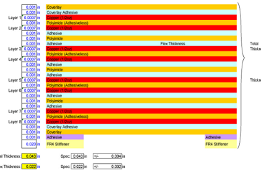
CAD tools allow detailed layer configuration, including thickness, copper weight, and dielectric constants. These values directly affect impedance, trace behavior, and overall board functionality. Ensure each layer serves a specific purpose to avoid unnecessary complexity.
Advanced CAD platforms also simulate thermal buildup and electromagnetic interference. These simulations help refine the HDI PCB design before prototyping. Good stackup planning minimizes crosstalk, improves manufacturability, and enhances board performance.
Accurate layer planning ensures each HDI PCB design supports reliable high-speed operation and compact architecture.
Define the Layer Stackup
A well-defined stackup ensures that signals remain stable and consistent. In HDI PCB design, each layer plays a critical role in routing, shielding, or power distribution. The choice of layer count affects both performance and manufacturing cost.
Define core and prepreg layers carefully to maintain structural integrity. For example, a 1-6-1 stackup includes microvias on outer layers and through vias in the core. This arrangement supports dense routing in HDI PCB Design without compromising reliability.
Use alternating signal and ground layers to reduce noise and crosstalk. Dedicated power and ground planes also help stabilize voltage levels during high-speed switching. CAD tools allow designers to model these layers and visualize current paths.
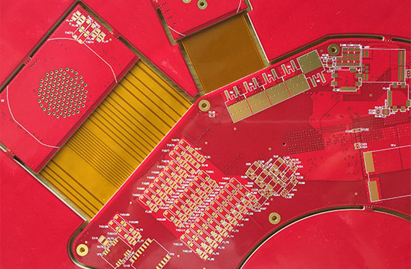
Be sure to include layers for mechanical strength if the board requires rigid or semi-flexible zones. These layers ensure durability, especially in mobile or aerospace applications.
Proper stackup planning enables smoother fabrication and results in a stable, high-performance HDI PCB Design.
Impedance Control
Controlling impedance is essential in high-speed HDI PCB design. Without it, signals may reflect or distort, leading to data loss or timing errors. CAD tools allow trace modeling to maintain controlled impedance throughout the layout.
Begin by defining target impedance values for signal types like USB, HDMI, or DDR. A 50-ohm single-ended trace or a 100-ohm differential pair is common. Trace width, spacing, and dielectric thickness all influence impedance.
Use built-in impedance calculators within the CAD software to adjust trace dimensions. Modify the stackup or material properties to meet specific design constraints. In HDI PCB design, precise trace tuning is critical for maintaining performance.
Simulate signal behavior across layers to verify impedance consistency. Mismatched impedance causes reflections that reduce data integrity. Tools like time-domain reflectometry (TDR) models can highlight problem areas before fabrication.
Managing impedance ensures signal quality and reliability in every HDI PCB design, especially in fast-switching or high-frequency applications.
Configuring HDI Via Types
Selecting the correct via types is essential in HDI PCB design. Different via structures serve unique purposes based on board density, signal performance, and manufacturing constraints. CAD tools enable designers to configure microvias, blind vias, buried vias, and via-in-pad structures accurately.
Each via type affects routing flexibility and signal behavior. Microvias are ideal for short connections between adjacent layers, while buried vias help avoid surface clutter. In complex HDI PCB Design, combining these vias allows for more compact and efficient layouts.
CAD platforms support custom via definitions and stack management. DRC flag potential spacing or alignment errors. This ensures each via meets fabrication standards and maintains reliability.
Proper via selection contributes to thermal relief, signal integrity, and board yield. In HDI PCB design, configuring vias strategically reduces congestion and supports high-speed routing. Effective use of via types leads to cleaner layouts and fewer assembly issues.
Microvias
Microvias are a core feature in compact HDI PCB Design. These vias connect adjacent layers using laser drilling, resulting in much smaller diameters than traditional mechanical vias. Their reduced size allows for tighter component placement and higher routing density.
Designers use CAD tools to position microvias between layer pairs like L1-L2 or L7-L8. This placement supports stacked or staggered via configurations. In multi-layer HDI PCB Design, stacking microvias increases vertical interconnect without consuming surface area.
CAD software helps manage the aspect ratio of microvias, which must remain within fabrication limits. A typical microvia might have a depth-to-diameter ratio of 1:1 or less. Exceeding this ratio can lead to reliability issues during HDI PCB Design.
Microvias also help manage impedance and thermal paths when strategically placed. Their minimal footprint supports denser routing under BGAs or fine-pitch components. Using microvias effectively enhances performance, manufacturability, and mechanical stability in advanced designs.
Blind and Buried Vias
Blind and buried vias are essential for multi-layer HDI PCB Design. These vias help route signals between non-adjacent layers while keeping surface layers clear. Blind vias connect outer layers to inner ones, while buried vias connect only internal layers.
CAD software allows precise placement and depth control of both types. This flexibility supports custom via stacks, reducing via stubs that cause signal reflections. For high-speed HDI PCB Design, minimizing stubs improves signal integrity and timing accuracy.
Using blind and buried vias also increases design real estate on surface layers. Designers can route sensitive traces away from noisy components or signals. This improves EMI control and overall electrical performance.
Manufacturing constraints must be considered when adding these vias to an HDI PCB Design. Each added drill step increases fabrication cost and complexity. When used strategically, blind and buried vias allow designers to balance performance with manufacturability.
Via-in-Pad Technology
Via-in-pad is a high-precision technique used in HDI PCB Design. It places vias directly beneath component pads, enabling ultra-compact layouts and direct routing. This method is especially useful under BGAs and fine-pitch ICs.
CAD tools allow via-in-pad placement with careful control of pad geometry and solder mask layers. Designers must also plan for via filling and plating, which ensures flat, solderable surfaces. In advanced HDI PCB Design, this reduces parasitic inductance and improves thermal conduction.
Via-in-pad helps eliminate long trace runs from fine-pitch packages. This lowers impedance mismatches and enhances high-speed signal paths. However, improper use can lead to solder voids or assembly defects.
Manufacturers may require filled and capped vias to ensure reliability. CAD systems include these fabrication details via definition. Using via-in-pad effectively allows designers to reduce board size, increase performance, and meet strict packaging requirements in modern HDI PCB Design.
Routing High-Speed Signals
Routing high-speed signals requires precision in every phase of HDI PCB design. Signal integrity issues such as reflections, delays, and ringing must be carefully managed. CAD software helps maintain optimal trace lengths, controlled impedance, and matched routing paths.
Designers should follow length-matching techniques and layer transitions with minimal stubs. For example, using short, direct traces reduces propagation delay and prevents timing skew. In HDI PCB design, high-speed signals often route through microvias to reduce loop areas.
Proper layer stacking and ground referencing are also crucial. CAD tools allow control via transitions and enable designers to visualize signal return paths. In complex HDI PCB design, simulations can verify timing and eye diagrams before fabrication.
Routing protocols like DDR, PCIe, or USB 3.0 benefit from pre-layout signal planning. Every trace layout impacts noise immunity and EMI. Applying structured high-speed routing ensures stable signal performance in advanced HDI PCB design applications.
Controlled Impedance Routing
Controlled impedance routing ensures that high-frequency signals behave predictably. In HDI PCB design, signal traces must match the impedance required by device specifications. CAD tools assist by calculating trace width, spacing, and layer stack parameters.
Designers use impedance calculators and field solvers to determine ideal trace geometries. For example, a 50-ohm single-ended trace may require exact width and clearance adjustments depending on the dielectric material. Maintaining consistent impedance throughout a trace’s path is critical in HDI PCB design.
Any discontinuities in impedance can cause signal reflections or losses. Controlled impedance techniques improve signal rise times, reduce jitter, and enhance overall data integrity. In HDI PCB design, these practices become essential for GHz-range applications.
CAD platforms support impedance-driven design rules and flag mismatches automatically. With the right configuration, layout engineers can route signals that comply with industry standards. Controlled impedance routing elevates the quality and performance of any HDI PCB design.
Differential Pair Routing
Differential pair routing involves two complementary signals routed side by side. In HDI PCB design, this technique helps maintain noise immunity and signal clarity. Pairs such as USB, LVDS, and HDMI require consistent spacing and length matching.
CAD software enables the creation of matched-length pairs and enforces uniform spacing rules. For example, if one trace is longer, it may introduce timing skew, degrading signal quality. In advanced HDI PCB design, designers must also avoid sharp bends and via mismatches.
To ensure signal integrity, keep both traces on the same layer whenever possible. Use tight coupling and proper return paths to suppress electromagnetic interference. Many HDI PCB design environments support auto-tuning features to assist with pair balancing.
Using differential routing effectively reduces common-mode noise and increases data transmission rates. Each routed pair contributes to system stability. When implemented correctly, differential pair routing is a foundational skill in high-speed HDI PCB design.
Minimize Crosstalk
Crosstalk occurs when a signal unintentionally interferes with adjacent traces. Reducing this effect is a major concern in HDI PCB design, especially in dense layouts. High-speed signals can induce voltage spikes in nearby lines without proper spacing.
To minimize crosstalk, increase spacing between aggressive and victim traces. Use ground shielding or guard traces to isolate high-speed lines. In HDI PCB design, layer stacking and reference planes also play key roles in electromagnetic control.
CAD tools allow engineers to define minimum trace separation and simulate coupling effects. For instance, placing a ground plane below critical traces can absorb stray signals. Reducing via transitions also limits exposure to noise paths in HDI PCB design.
Consider using differential pairs and controlled impedance to naturally reduce interference. Each layout decision affects signal quality and board reliability. Implementing crosstalk control techniques is essential to ensure dependable performance in advanced HDI PCB design projects.
Placing Components for HDI Design
Smart component placement is critical to successful HDI PCB design. Compact layouts require precision when positioning connectors, ICs, and decoupling capacitors. CAD tools assist by aligning parts with routing channels and minimizing via usage.
For example, placing high-speed components near signal exits reduces trace lengths and delays. Grouping related parts—such as clock sources with processors—enhances signal synchronization. In complex HDI PCB design, even minor placement changes can affect signal flow.
Top-layer real estate is limited, so prioritize essential components near the center. Use inner layers and microvias to connect BGA pins efficiently. CAD platforms support 3D visualization, helping engineers check clearances and stacking.
Proper placement also improves thermal dissipation and power delivery. In HDI PCB design, balancing signal paths and power planes requires careful spacing. Aligning functionality with layout constraints makes the design process smoother and more efficient for final fabrication.
Optimize Component Placement
Optimizing placement starts with understanding electrical, mechanical, and thermal needs. In HDI PCB design, placing power-hungry components near regulators reduces voltage drop. CAD software enables designers to simulate thermal effects and rework layouts early.
High-speed components should have direct routes to connectors or terminations. For instance, placing DDR memory close to the processor improves signal timing. Proper spacing between analog and digital circuits minimizes interference.
Additionally, arranging decoupling capacitors as close as possible to power pins improves transient response. CAD tools allow pin swapping and footprint editing to refine layout. In any HDI PCB design, placement decisions impact routing efficiency and signal integrity.
Using hierarchical blocks or placement templates can speed up the process. These tools reduce errors and save valuable board space. With optimized layouts, engineers reduce rework, shorten development cycles, and enhance overall product reliability in HDI PCB design projects.
Use Designators and Nets
Clear labeling improves traceability and speeds up layout reviews. In HDI PCB design, using consistent designators for each component helps during routing. CAD software assigns unique identifiers, making it easier to troubleshoot or modify designs.
Net assignments define the electrical connections between parts of the circuit. Assigning meaningful names—such as “VCC_Core” or “CLK_100MHz”—clarifies routing paths. Well-named nets reduce confusion, especially in multi-layer or dense HDI PCB design projects.
Tools like net classes and custom filters help isolate signal groups. This allows designers to route differential pairs, power, and analog lines independently. In professional HDI PCB design, these practices simplify team collaboration and manufacturing handoffs.
Labeling also aids in documentation and version control. Each change becomes easier to track and verify through design history. When used properly, designators and nets create structure and clarity throughout the entire HDI PCB design process.
Routing Strategies for HDI Designs
Designing for high-density interconnect boards demands advanced layout techniques. CAD software provides critical tools for managing constraints, microvias, and fine-pitch components. These technologies allow engineers to build compact, high-speed, and multi-layer designs efficiently.
HDI PCB design introduces unique challenges such as tight spacing, controlled impedance, and heat distribution. CAD platforms offer interactive routing, auto-routing suggestions, and layer stack configuration. Mastery of these tools enables precise, rule-driven design development.
Understanding HDI PCB design from concept to fabrication saves time and cost. Simulation tools integrated in CAD platforms help catch design flaws early. With proper planning and skillful execution, designers can achieve higher performance and reliability.
Fan-Out for BGAs
Ball Grid Arrays (BGAs) present routing difficulties in HDI PCB design. Fan-out strategies involve placing vias in-pad or near-pad to connect inner layers. CAD software automates this process, saving time and ensuring spacing accuracy.
To reduce congestion, designers often stagger microvias or use via-in-pad techniques. This enables escape routing for fine-pitch packages like FPGAs and processors. Proper fan-out allows for easier routing on adjacent layers and minimizes signal distortion.
Effective fan-out planning directly influences signal integrity and board manufacturability. Many CAD tools provide escape routing wizards for complex BGA configurations. In modern HDI PCB design, this feature is essential to maintain performance in miniaturized layouts.
Via Management
Efficient via management plays a critical role in HDI PCB design. Using blind, buried, and microvias allows designers to create dense interconnects without consuming surface space. CAD tools allow the configuration of stacked and staggered vias with controlled dimensions.
Improper via usage can cause manufacturing issues or signal loss. For instance, thermal relief or incorrect aspect ratios lead to structural failures. Advanced CAD software ensures via optimization layer-by-layer via modeling.
In HDI PCB design, well-managed vias reduce EMI, improve current flow, and enhance signal timing. By setting via constraints and rules early, designers prevent costly revisions later. Intelligent via planning increases both electrical and mechanical stability.
Signal Path Optimization
Optimizing signal paths is vital for performance in HDI PCB design. Shorter trace lengths reduce propagation delay and minimize crosstalk. CAD tools assist with length matching and impedance control, especially for high-speed differential pairs.
To maintain timing integrity, match signal paths in memory interfaces, such as DDR or PCIe lanes. Routing signals on adjacent layers with ground shielding reduces noise. Proper topology choices—like point-to-point or daisy chain—enhance communication accuracy.
Using CAD software to simulate signal behavior prevents failure under real-world conditions. Signal path tuning features allow real-time adjustment during layout. Optimized paths result in lower jitter and improved data integrity across the HDI PCB design.
Thermal Management in CAD Software
Effective thermal management is essential when designing high-performance electronic circuits. Without it, components overheat, reducing reliability and shortening product lifespan. Modern PCB CAD software enables designers to identify, simulate, and resolve thermal issues during early development stages.
Thermal analysis tools within PCB CAD software visualize heat distribution across layers. These simulations help ensure critical components like voltage regulators and power ICs stay within safe temperature ranges. Managing heat flow reduces risk in densely packed HDI layouts.
Using PCB CAD software to plan heat sinks, copper pours, and airflow improves thermal performance. These features offer real-time insights, allowing quicker design iterations. With precise control over thermal behavior, engineers create more efficient and durable HDI boards.
Thermal Vias
Thermal vias help transfer heat from surface-mounted components to internal copper planes. These small, strategically placed holes conduct heat vertically through the PCB layers. In power-dense areas, using a grid of thermal vias ensures better heat dissipation.
PCB CAD software allows precise placement and quantity control for thermal vias. Designers can model thermal vias directly beneath heat-generating components like FETs or power amplifiers. This placement maximizes contact with internal ground or power planes.
Spacing, via size, and pad connection significantly affect thermal transfer efficiency. Using thermal relief patterns around vias balances heat flow and soldering quality. Advanced PCB CAD software even calculates optimal via patterns for complex thermal challenges.
Thermal Simulation
Thermal simulation in PCB CAD software predicts how heat behaves under real-world conditions. Engineers can input power consumption, material properties, and ambient temperature to model heat generation. The simulation maps hot spots, thermal gradients, and airflow interaction.
Identifying these zones early helps guide design improvements like sink placement or trace width adjustment. PCB CAD software enables what-if testing—such as changing board thickness or adding copper areas—without physical prototypes. These tools accelerate time-to-market by eliminating guesswork.
Reliable thermal simulation ensures compliance with safety and performance standards. It also supports certification processes, such as UL or IPC guidelines. By integrating thermal modeling into the workflow, PCB CAD software empowers engineers to design robust, high-efficiency HDI systems.
Design Rule Checks (DRC)
Design Rule Checks (DRC) are essential for ensuring layout compliance. DRC validates spacing, trace width, via size, and clearance rules before manufacturing. Modern PCB CAD software automates these checks to reduce human error.
Without DRC, minor violations can cause board failure or short circuits. Every step in PCB CAD software—from layer stack-up to routing—is governed by defined constraints. This process guarantees designs meet both fabrication and functional requirements.
Comprehensive DRC tools within PCB CAD software allow immediate error identification. Designers can resolve violations quickly, saving time and costly rework. Efficient use of DRC results in cleaner, more reliable HDI boards.
Set Design Constraints
Setting design constraints is the foundation of a successful HDI layout. Constraint settings define how close traces can run or how wide they must be. These include via sizes, trace widths, impedance targets, and clearance to copper features.
With PCB CAD software, engineers create rule sets for specific layers or nets. High-speed signals may need tighter spacing control or matched lengths. Constraint-driven design ensures the board meets electrical, mechanical, and thermal goals.
Clearly defined constraints enable faster DRC and fewer manual edits. Teams working on complex HDI PCB projects benefit from consistent design standards. Most PCB CAD software platforms offer constraint templates that reduce setup time.
Run Automated DRC
Automated DRC is a core feature in modern PCB CAD software. It scans the entire board for violations against the defined design rules. This automation catches spacing errors, unconnected nets, and improper via placement.
Running DRC frequently during layout helps spot issues early. For example, it can detect traces routed too close to drill holes or pads. Using PCB CAD software in this way minimizes surprises during final verification.
The tool often highlights errors with detailed messages or interactive markers. With each pass, the layout improves in both compliance and performance. Ultimately, automated DRC boosts design speed and accuracy significantly.
Simulation and Validation
Simulation and validation are critical steps after completing the initial layout. These tools model how the HDI board will perform under electrical loads. PCB CAD software often includes integrated simulators for real-time feedback.
For instance, signal reflection, crosstalk, and impedance mismatches can be predicted. Designers can then refine trace geometry or layer stack-ups. Using PCB CAD software for simulation reduces the need for multiple prototypes.
Validation also involves checking mechanical constraints, clearances, and thermal response. By running simulations early, engineers ensure functionality before production. This proactive approach enhances both quality and reliability.
Signal Integrity Simulation
Signal integrity simulations evaluate how electrical signals behave across the PCB. High-speed traces are sensitive to reflections, delays, and electromagnetic interference. PCB CAD software helps visualize these behaviors and pinpoint problem areas.
Engineers use it to analyze transmission lines and trace lengths via stubs. Adjustments like tuning trace widths or adding terminations often follow. The simulation ensures signals reach destinations cleanly and without distortion.
Accurate modeling prevents costly late-stage failures in complex HDI designs. Signal integrity tools in PCB CAD software are essential for high-frequency and differential pair layouts. They ensure compliance with industry standards like PCIe or USB.
Power Integrity Analysis
Power integrity ensures stable voltage delivery throughout the circuit board. It examines how power planes and decoupling capacitors handle transient demands. PCB CAD software includes tools for analyzing voltage drop and noise levels.
For example, excessive IR drop on thin power traces can degrade IC performance. Engineers model current paths and optimize via arrays or copper pours. The result is cleaner power delivery and reduced EMI issues.
Power integrity tools within PCB CAD software assist in selecting proper bypass caps. They also help with strategic placement near critical components. Well-managed power paths improve reliability in dense HDI layouts.
3D Visualization
3D visualization offers a complete view of the assembled PCB. This feature shows component height, alignment, and enclosure fit. Using PCB CAD software, engineers inspect every detail before fabrication.
Visualizing in 3D helps detect overlapping components or incorrect orientations. It’s especially useful when dealing with tight enclosures or stacked connectors. PCB CAD software also generates step files for mechanical collaboration.
In addition, 3D tools aid in verifying layer transitions and via paths. This ensures that critical signals don’t intersect with mechanical constraints. Designers using PCB CAD software gain better spatial awareness and layout confidence.
Exporting Files for Manufacturing
Exporting files correctly is essential for transitioning from digital designs to physical boards in HDI PCB assembly. CAD tools make it possible to compile all necessary data into precise output files, ensuring manufacturers receive accurate instructions. Errors in exported files can result in production delays, costly revisions, or non-functional boards.
Proper use of CAD platforms helps avoid these pitfalls by supporting formats tailored to advanced board manufacturing. For HDI PCB assembly, attention to details like layer stacks, drill information, and netlists ensures every design feature is preserved. Consistency between what’s designed and what gets built relies heavily on exporting clean, complete, and compatible data.
Therefore, designers must understand what files are needed, when to generate them, and how to ensure file integrity. With HDI technology becoming more widespread, exporting with precision is no longer optional—it’s a foundational skill for successful hardware development.
Generate Manufacturing Files
One of the most critical tasks in HDI PCB assembly is generating the correct manufacturing files. CAD tools are typically equipped with features to output Gerber files, drill files, pick-and-place data, and a Bill of Materials (BOM). Gerber files, in particular, represent the visual layers of the board, such as copper, solder mask, and silkscreen.
Drill files define the sizes and locations of all via and hole placements. BOMs must be carefully curated to list correct part numbers, values, and packages. Pick-and-place files guide automated machines during component population, reducing manual error.
Using PCB CAD software efficiently allows designers to generate these outputs consistently and accurately. For example, platforms like Altium Designer and KiCad include automated file export utilities that cross-check for missing information. These functions help reduce revision cycles and keep projects on track. Proper file generation lays the foundation for a seamless and cost-effective HDI PCB assembly process.
Panelization
Panelization is essential when designing boards for high-volume HDI PCB assembly. This process groups multiple copies of the same PCB onto a single manufacturing panel, improving fabrication efficiency and material utilization.
CAD tools allow users to define spacing, breakaway tabs, fiducials, and tool holes—elements critical to automated assembly lines. Well-executed panelization minimizes handling time, reduces board waste, and supports machine alignment during population and soldering.
For instance, adding mouse bites or V-score lines enables easy board separation after assembly without damaging edge components.
Most PCB CAD software platforms include built-in panelization tools that allow users to preview layout arrangements in real time. These features help evaluate whether the design meets manufacturing tolerances and minimizes routing constraints. Panel optimization also affects thermal distribution and process yield. Understanding panelization is vital not only for layout engineers but also for production managers aiming to streamline HDI PCB assembly workflows and reduce unit costs.
Output IPC-2581 or ODB++ Files
When preparing a design for HDI PCB assembly, choosing the right output format is just as important as the design itself. IPC-2581 and ODB++ formats offer intelligent, comprehensive data structures that go far beyond standard Gerber files. These formats include layer stackups, netlists, fabrication notes, and assembly instructions—all bundled into a single digital container. Outputting IPC-2581 or ODB++ using PCB CAD software reduces communication errors with manufacturers and eliminates file misinterpretation.
For example, IPC-2581 enables end-to-end traceability, which supports faster debugging and higher process quality. CAD tools such as Mentor Xpedition, Altium, and Cadence Allegro support native export of both formats, helping teams integrate seamlessly with global fabricators. This is particularly useful in HDI PCB assembly, where dense routing, microvias, and fine-pitch components leave no room for interpretation.
Moving to intelligent data formats not only streamlines fabrication but also strengthens design reliability and lifecycle documentation. This ensures efficient, repeatable results for complex HDI builds.
Best Practices for HDI PCB Design in CAD
Designing for HDI PCB assembly demands strict attention to detail and process discipline. Unlike standard boards, HDI layouts involve microvias, thinner traces, and tighter tolerances that challenge both software and hardware limits.
CAD tools provide the flexibility needed to define fine-pitch BGA footprints, stacked via structures, and controlled impedance lines. Implementing best practices ensures signal integrity, manufacturability, and electrical performance remain intact.
Every stage—from schematic capture to output file generation—must follow a logical, consistent flow. Using layer stack managers and design rule checks (DRCs) inside CAD software helps avoid critical errors. For example, defining via-in-pad guidelines early reduces rework during HDI PCB assembly.
Aligning the design process with proven standards streamlines communication and reduces risk. Without following best practices, small mistakes can result in major functional failures during testing or production. Clear planning and execution make the difference between a working prototype and a costly redesign.
Collaborate with Manufacturers
Effective collaboration with fabrication and assembly partners improves the success rate of HDI PCB assembly. Manufacturers often provide design guidelines tailored to their equipment capabilities and process limits. CAD tools should be configured to reflect these constraints from the start. For instance, adjusting minimum trace widths or via diameters according to shop specifications avoids redesign delays.
Early engagement allows both parties to review stackups, discuss material choices, and identify possible bottlenecks. Many CAD platforms allow importing design rules directly from manufacturers to enforce compliance. Incorporating these into the initial layout minimizes the need for revisions.
Working closely with a manufacturing partner also helps select the correct type of laser-drilled vias or buried via configurations. Since HDI boards rely heavily on high-density interconnects, production feedback is essential to avoid yield issues. Keeping this communication loop active throughout the process increases reliability and reduces rework. Collaborating properly supports smoother HDI PCB assembly execution and faster time-to-market.
Iterative Prototyping
Iterative prototyping is essential when working with advanced HDI PCB assembly. Complex designs benefit from multiple review and build cycles to uncover layout flaws or manufacturing risks. Using CAD software, engineers can create early prototypes with limited layer counts to test critical functions. These builds reveal potential issues such as impedance mismatches, crosstalk, or signal degradation.
Design simulation features within CAD tools allow validation of these behaviors before physical fabrication. Each iteration should refine via placement, routing constraints, and component spacing. For example, moving a decoupling capacitor closer to a processor can reduce power noise. Iterative design also helps identify heat dissipation problems in densely packed areas.
By testing partial or scaled-down versions, layout engineers gain clarity before finalizing the entire build. These prototypes provide data to adjust stackups, materials, or trace widths for the final HDI PCB assembly. Without iterative testing, the risk of field failures or functional breakdown increases significantly. CAD-assisted prototyping remains one of the most reliable methods for optimizing complex electronics.
Keep Documentation Updated
Maintaining up-to-date design documentation is critical to a successful HDI PCB assembly process. Documentation includes fabrication drawings, layer stackups, assembly notes, test points, and revision history. CAD software enables auto-updating of these files when layout changes occur, reducing manual oversight. Inconsistent documentation often leads to delays, incorrect builds, or QA failures during production. For example, failing to update via specifications on the fabrication notes may result in the wrong drill size being used.
Annotated schematics and updated bills of materials (BOMs) ensure all stakeholders remain aligned. Revision control systems inside CAD platforms help track each change, enabling traceability and accountability. Accurate records also assist in product certifications and future redesigns.
Regular updates support compliance with IPC standards and manufacturer guidelines, both of which are crucial in HDI PCB assembly workflows. Poor documentation creates bottlenecks between teams and introduces ambiguity into critical processes. Keeping all files synchronized ensures reliability, repeatability, and long-term design efficiency.
Final Remarks
Designing for HDI PCB assembly using CAD software is both a technical and strategic process. Success depends on applying best practices, leveraging collaborative input, and using tools efficiently. Each step—from initial schematic capture to exporting final manufacturing files—requires thoughtful planning and disciplined execution. Working closely with manufacturers ensures alignment on tolerances, material selections, and via structures. Through iterative prototyping, engineers can refine designs based on real-world performance data before committing to full-scale production.
CAD platforms support this process with simulation tools, stackup managers, and automated DRCs tailored for HDI complexity. Equally important is maintaining updated documentation that accurately reflects all changes and design decisions. Clear, current files prevent miscommunication during fabrication and improve quality assurance outcomes.
With advanced features and proper workflows, CAD software becomes more than just a layout tool—it’s an essential part of the HDI PCB assembly pipeline. The increasing demand for compact, high-performance electronics makes mastering HDI design skills more valuable than ever.
Engineers who prioritize precision, communication, and documentation will be better equipped to deliver reliable products on time and within budget. By following the methods outlined above, teams can confidently navigate the challenges of HDI PCB design and bring sophisticated hardware solutions to life.

![Understanding PCB Costs & Pricing [Your Complete Guide] Understanding PCB Costs & Pricing [Your Complete Guide]](https://hdicircuitboard.com/wp-content/uploads/elementor/thumbs/Understanding-PCB-Costs-Pricing-Your-Complete-Guide-qzzhe6mcaxuolkux3xalfktgavumi9y1aqfbs9bpv4.webp)
