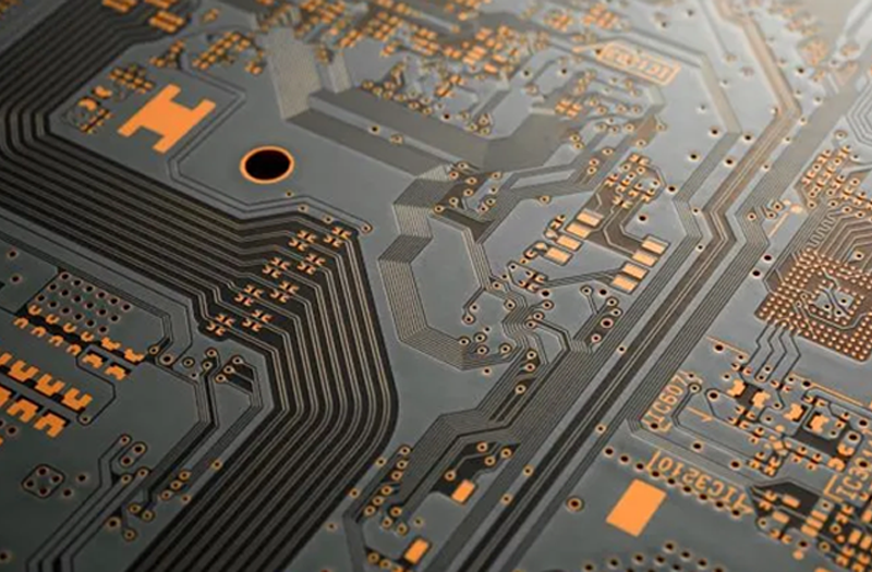
High-Density Interconnect (HDI) PCBs have revolutionized the electronics industry by enabling smaller, faster, and more reliable devices. These boards demand advanced fabrication techniques for HDI PCBs to achieve their intricate designs, ultra-fine traces, and dense component placement.
The power sector of the electronics industry depends on HDI PCBs to operate smartphones together with medical devices. HDI fabrication techniques for PCBs need to use manufacturing approaches which challenge the boundaries of both refinement and material expertise and production engineering capabilities.
Stacking microvias alongside embedded components and layered constructions enables HDI PCBs to enhance signal clarity thus achieving smaller designs while managing equipment heat better. The growing market need for compact high-performance devices requires printed circuit board manufacturing to implement advanced production methods for staying competitive.
Today, we will consider the modern innovations in HDI PCB production while discussing manufacturing obstacles and substance selection alongside processing techniques which lead to enhanced performance in contemporary high-tech equipment.
The Latest Advancements in HDI PCB Fabrication Techniques
HDI PCB fabrication techniques now prioritize three main areas which include:
- Signal integrity
- Reliability and
- Miniaturization.
The three methods of laser drilling, together with sequential lamination and direct imaging, have become essential procedures in PCB production to create microvias and ultra-fine traces. The incorporation of passive elements and 3D layered construction results in smaller boards that deliver upgraded functions. The recent technological advances allow printed circuit board producers to satisfy requirements in contemporary electronic products that demand both compact designs and high performance.
AOI systems with defect detection enabled by artificial intelligence allow printed circuit board manufacturers to maintain precision in high-density board designs in their manufacturing process. The performance of high-frequency applications benefits from low-loss dielectrics and high-temperature laminates which are advanced materials.
The signal loss reduction in 5G and IoT devices depends more and more on materials like Rogers 4000 and Isola Astra. The technological progress enables PCB board manufacturers to create boards with more reliability and efficiency while maintaining compact dimensions.
The PCB manufacturing process has been revolutionized through the introduction of inkjet printing as an additive manufacturing technology. Powerful deposition of conductive materials by this method lowers production timelines while minimizing waste streams. The speed and economic efficiency of PCB printed circuit board assembly processes has improved due to which manufacturers can handle escalating high-performance electronics market requirements.
How Does Laser Drilling Improve HDI PCB Fabrication?
Laser drilling serves as an essential technology for producing High Density Interconnect PCBs. Laser drilling technology produces microvias with diameters down to 25µm which traditional mechanical drills cannot match because of their limited capability to drill below 100µm. The high degree of precision in laser drilling represents a fundamental requirement for producing essential blind and buried vias in multilayer designs that support high-density interconnects.
The manufacturing process of PCBs uses lasers to vaporize copper and dielectric material through non-damaging processes which minimizes delamination risks. The laser industry typically employs CO2 and UV devices for manufacturing purposes yet UV lasers show superior performance in detailed applications since their wavelength is shorter.
Higher aspect ratios become achievable through this technique while maintaining system integrity during deep via creation. Printed circuit board manufacturers who use laser drilling technology can generate increased interconnect density required for modern PCB circuit board manufacturing.
Through laser drilling manufacturers can produce intricate designs of staggered and stacked microvias due to its increased design flexibility. The compact design of signals depends on these vital structures which find extensive use in smartphones and wearables.
Through its precise drilling method, laser technology makes post-processing unnecessary, which leads to decreased time and manufacturing expenses during PCB production.
What Are the Challenges of Via Filling in HDI PCBs?
The production of HDI PCBs requires success via filling as a fundamental yet difficult fabrication process. Electronic and mechanical stability during manufacturing requires filling microvias with conductive or non-conductive pastes. However, air bubbles, incomplete filling, and material shrinkage can compromise reliability, leading to potential failures in the final product.
The production of PCB boards involves vacuum-assisted filling systems with low-viscosity epoxy resins as a solution for addressing these concerns. The use of conductive pastes with silver or copper nanoparticles enhances conductivity yet needs exact curing procedures to prevent void formation.
The use of non-conductive fills remains cost-efficient but requires perfect planarization because any imperfections could result in uneven surfaces during lamination. Cross-sectional analysis serves as part of rigorous testing to verify the integrity of vial openings in the PCB circuit board assembly which protects against hidden defects.
The manufacturing process of PCBs presents difficulties in managing thermal properties of filled vias. Lamination heat exposure makes filling materials expand which results in both cracks and delamination defects. Manufacturers address this issue through their selection of thermal expansion low materials and optimized curing processes for maintaining uniform filling. The implementation of these measures ensures reliable performance in demanding applications for HDI PCBs.
The Role of Microvia Technology in HDI PCB Design a
Manufacturers utilize microvia technology as the fundamental basis for building HDI PCBs. The small interlayer connections known as microvias measure between 50–150µm in diameter to link vertical paths without occupying too much space. The ability to arrange microvias in stacked and staggered formations enables designers to create intricate signal routes in small board layouts which benefit wearable technology devices while benefiting aerospace systems.
The electrical connection between external and internal board layers happens through blind microvias while buried vias establish connections between intermediate layers to shorten signal travel distances. The decreased parasitic capacitance and inductance makes high-speed performance possible.
Printed circuit board assembly through PCB uses microvias for accommodating BGA components which establishes dependable solder connections and thermal regulation.
Electronic devices continue to shrink in size because microvia technology serves this miniaturization movement. The high density connections made possible by microvias enable designers to integrate more board functions into compact board dimensions.
The compact nature of medical devices and IoT sensors requires microvias to be essential because space availability is limited. The PCB manufacturing industry advances through innovation because microvia technology serves as its principal enabling technology.
How Do Advanced Imaging Techniques Improve HDI PCB Quality?
Laser direct imaging (LDI) serves as an advanced imaging technology which revolutionized the fabrication methods for high-density interconnect PCBs. The UV laser technology of LDI exposes photoresist material with precise micrometer accuracy to prevent traditional photolithography alignment errors. The fabrication of ultra-fine traces below 40µm as well as high-density designs, depends on this technique.
AOI systems using high-resolution cameras and machine learning algorithms perform early PCB defect detection of opens and shorts and misregistrations throughout the manufacturing process. The systems perform design file comparison for printed circuit boards to identify any inconsistencies which can be identified early and prevented from worsening. Printed circuit board manufacturers achieve exactness across manufacturing phases to produce PCB circuit boards that fulfill strict quality standards.
The use of 3D X-ray imaging technology has risen to perform inspections of hidden features including buried vias and solder joints. The non-destructive testing method delivers detailed board internal inspection results which help to verify complex design quality standards. The advanced imaging methods play a critical role in both reliability and performance maintenance of HDI PCBs when used in demanding applications.
Benefits of Embedded Components in HDI PCB Fabrication
HDI PCB fabrication techniques benefit tremendously from the integration of passive or active components inside PCB layers. The method decreases the available surface area and shortens electrical pathways while reducing unwanted effects. HDI PCB fabrication allows resistors, capacitors and even ICs to be concealed between layers which creates space for more routing elements and components.
Embedded components used in PCB printed circuit board assembly help increase reliability because they protect sensitive components from environmental stressors. The electrical performance in high-frequency designs improves due to their ability to minimize crosstalk and impedance mismatches. Accurate placement and bonding procedures must be performed to prevent board delamination during the lamination process.
Embedded components enhance thermal management as their main benefit. Heat-generating components inside the board structure enable manufacturers to spread heat evenly which decreases hotspot formation.
This is particularly important for high-power applications like automotive electronics and data centers. As a result, embedded components are becoming a key feature of advanced HDI PCB designs.
Optimizing HDI PCB Fabrication for High-Frequency Designs
The optimization process for high-speed applications of HDI PCB production relies on selecting materials controlling impedances, and managing signal integrity. Rogers 4000 together with Isola Astra represent low-loss dielectric materials that maintain signal quality during GHz frequency operations.
Accurate management of impedance between traces becomes possible by maintaining exact spacing and width dimensions which eliminates signal reflections and timing discrepancies. Ground planes together with shielding vias help minimize electromagnetic interference (EMI).
PCB board producers employ simulation platforms to examine signal behavior which allows them to optimize designs before starting production. PCB circuit board assemblies achieve 5G and radar and high-performance computing requirements through these implementation strategies.
The signal distortion can be minimized through the implementation of advanced via structures which include back-drilled vias and via-in-pad designs. Back-drilling the unused areas of plated holes eliminates stub effects which harm signal quality.
With via-in-pad design standards manufacturers implement pads directly above vias which creates shorter signal paths that lead to better system performance. Modern electronics need these techniques as an essential requirement to reach their required high-speed performance levels, such as in space.
What Are the New Materials Used in HDI PCB Fabrication?
The development of new materials has transformed the methods used for creating HDI PCBs. The use of halogen-free laminates together with flexible substrates and thermally conductive dielectrics provides solutions to environmental forces and mechanical requirements and thermal management needs.
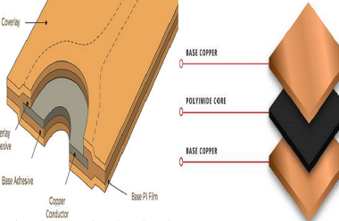
Polyimide films serve as flexible substrates for HDI technology to manufacture foldable electronics thereby ceramic-filled resins act as thermal dissipators in power-dense systems.
Low-CTE materials stop PCB printed circuit board assemblies from warping when they experience temperature variations which is essential for automotive applications. The use of nanocomposite coatings provides outstanding moisture protection which significantly increases the operational time of circuit boards within high-humidity environments.
The combination of laminates with added graphene creates new materials that provide top-level thermal and electrical conductivity. The materials find their best use in high-frequency applications because they excel at maintaining signal integrity and dissipating heat effectively. Next-generation electronics require specific needs which PCB board manufacturers achieve by implementing these innovative materials.
What Are the Advanced Lamination Techniques for HDI PCBs?
A high-speed HDI PCB fabrication requires selecting proper materials and controlling impedance while implementing signal integrity management techniques. Rogers 4000 together with Isola Astra represent low-loss dielectric materials that maintain signal quality during GHz frequency operations.
Accurate management of impedance between traces becomes possible by maintaining exact spacing and width dimensions which eliminates signal reflections and timing discrepancies. Ground planes together with shielding vias help minimize electromagnetic interference (EMI).
PCB board producers employ simulation platforms to examine signal behavior which allows them to optimize designs before starting production. PCB circuit board assemblies achieve 5G and radar and high-performance computing requirements through these implementation strategies.
The signal distortion can be minimized through the implementation of advanced via structures which include back-drilled vias and via-in-pad designs. Back-drilling the unused areas of plated holes eliminates stub effects which harm signal quality. With via-in-pad design standards manufacturers implement pads directly above vias which creates shorter signal paths that lead to better system performance. Modern electronics need these techniques as an essential requirement to reach their required high-speed performance levels.
How Can the HDI PCB Manufacturing Process Be Accelerated?
The development of new materials has transformed the methods used for creating HDI PCBs. The use of halogen-free laminates together with flexible substrates and thermally conductive dielectrics provides solutions to environmental forces and mechanical requirements and thermal management needs.
Polyimide films enable the production of foldable electronic devices through flexible HDI PCBs and ceramic-filled resins provide effective heat dissipation for power-dense applications.
Low-CTE materials stop PCB printed circuit board assemblies from warping when they experience temperature variations which is essential for automotive applications. Nanocomposite coatings provide exceptional moisture resistance that extends the operational lifetime of circuit boards when operating in humid environments.
The combination of laminates with added graphene creates new materials that provide top-level thermal and electrical conductivity. The materials find their best use in high-frequency applications because they excel at maintaining signal integrity and dissipating heat effectively.
Next-generation electronics require specific techniques which PCB board manufacturers achieve by implementing these innovative materials.
Advantages and Disadvantages of Stacked vs. Blind Microvias
Stacked microvias offer higher density by aligning vias vertically across layers, ideal for complex interconnects. However, they require precise alignment and increase the risk of thermal stress fractures. Blind microvias, connecting outer to inner layers, simplify manufacturing but limit routing flexibility. PCB board manufacturers often combine both types to balance density and reliability, ensuring robust PCB circuit board assemblies.
One advantage of stacked microvias is their ability to support higher layer counts, making them ideal for complex designs. However, their increased complexity can lead to higher production costs. Blind microvias, on the other hand, are more cost-effective but may not be suitable for the most demanding applications. By carefully selecting the appropriate via structure, manufacturers can optimize the performance and cost of HDI PCBs.
Advanced fill materials and via-in-pad designs mitigate the weaknesses of both types of microvias. For example, conductive fills improve electrical performance, while non-conductive fills enhance mechanical stability. These techniques ensure that HDI PCBs meet the stringent requirements of modern electronics, from smartphones to aerospace systems.
How Are 3D Stacked PCBs Fabricated for HDI Designs?
3D stacked PCBs involve bonding multiple HDI boards vertically using through-silicon vias (TSVs) or interposers. This technique maximizes space efficiency and shortens signal paths, crucial for memory modules and AI accelerators. The fabrication process requires ultra-thin dielectrics and precise alignment systems to ensure electrical continuity, making it a complex but rewarding endeavor for PCB board manufacturers.
Thermal management becomes critical in 3D stacked PCBs, necessitating advanced cooling solutions like microfluidic channels or thermally conductive adhesives. These measures prevent overheating and ensure reliable performance in high-power applications.
Additionally, 3D stacked PCBs enable the integration of heterogeneous components, such as processors and memory, into a single package. This reduces latency and improves performance, making them ideal for high-performance computing and data center applications.
The use of advanced materials, such as low-CTE laminates and flexible substrates, further enhances the reliability of 3D stacked PCBs. These materials can withstand the mechanical stresses associated with stacking, ensuring long-term durability. As a result, 3D stacked PCBs are becoming a key technology in the evolution of HDI PCB fabrication.
What Are the Most Advanced Soldering Techniques for HDI PCBs
Laser soldering and vacuum reflow are leading techniques in PCB printed circuit board assembly for HDI designs. Laser soldering targets specific joints with minimal heat spread, protecting sensitive components. Vacuum reflow eliminates voids in solder joints, enhancing mechanical and electrical reliability. These methods ensure high-yield assembly of printed circuit board PCBA units, even in densely packed layouts.
For ultra-fine-pitch components, solder jetting deposits precise amounts of solder paste, reducing bridging risks. This technique is particularly useful for HDI PCBs with high-density interconnects, where even minor errors can lead to failures.
Another advanced technique is the use of low-temperature solders, which reduce thermal stress on components and substrates. This is particularly important for HDI PCBs with embedded components, where excessive heat can cause delamination.
With the help of these advanced soldering techniques, manufacturers can produce reliable and high-performance HDI PCBs. These methods not only improve the quality of the final product but also reduce production costs by minimizing rework and scrap.
What Is the Impact of High-Density Interconnects on PCB Reliability?
High-density interconnects (HDIs) introduce reliability challenges like thermal stress, signal crosstalk, and mechanical fatigue. However, advanced fabrication techniques for HDI PCBs mitigate these risks. Reliable via filling, low-CTE materials, and conformal coatings enhance durability, ensuring that HDI PCBs can withstand the rigors of real-world applications.
Rigorous testing, including thermal cycling and vibration tests, validates PCB circuit board assemblies under real-world conditions. These measures ensure HDI PCBs meet the longevity demands of aerospace, medical, and automotive applications.
Additionally, the use of advanced materials like high-Tg laminates and flexible substrates improves the mechanical stability of HDI PCBs. These materials can withstand harsh environments, ensuring reliable performance over the lifespan of the product.
Another critical factor is the design of the interconnects themselves. By optimizing the layout and using advanced simulation tools, manufacturers can minimize signal loss and crosstalk, ensuring clean and reliable transmission. These strategies make HDI PCBs increasingly reliable, even in the most demanding applications.
Impact of Advanced PCB Fabrication Techniques to Signal Integrity
Signal integrity in HDI PCBs hinges on controlled impedance, reduced crosstalk, and minimized losses. Advanced fabrication techniques like laser-etched trenches and differential pair routing maintain consistent trace characteristics. Embedded planar capacitors decouple power supplies, reducing noise and ensuring clean signal transmission.
Simulation-driven design adjustments, such as optimizing via stubs and return paths, further enhance performance. These practices ensure PCB printed circuit board assemblies deliver clean signals in high-speed applications. Another critical factor is the use of advanced materials with low dielectric constants and loss tangents. These materials minimize signal attenuation, ensuring that high-frequency signals remain intact.
With these techniques, manufacturers can produce HDI PCBs with exceptional signal integrity, meeting the demands of modern electronics. These advancements are particularly important for applications like 5G networks and high-performance computing, where signal integrity is paramount.
What Are the Advanced Surface Finishing Options for HDI PCBs?
Surface finishes like ENEPIG (Electroless Nickel Electroless Palladium Immersion Gold) and immersion silver protect HDI PCBs from oxidation while enhancing solderability. ENEPIG offers superior durability for multiple reflow cycles, ideal for complex PCB assembly processes.
Organic solderability preservatives (OSP) provide a cost-effective, eco-friendly option for consumer electronics.
Another advanced option is the use of immersion tin, which provides a flat surface for fine-pitch components. This finish is particularly useful for HDI PCBs with high-density interconnects, where even minor surface irregularities can cause issues. By selecting the appropriate surface finish, manufacturers can ensure the reliability and performance of HDI PCBs in a wide range of applications.
Each finish is chosen based on application requirements, balancing cost, performance, and environmental factors. These advanced surface finishing options not only improve the functionality of HDI PCBs but also extend their lifespan, ensuring long-term reliability.
Conclusion
Advanced fabrication techniques for HDI PCBs are critical for meeting the demands of next-generation electronics. From laser drilling and microvia technology to innovative materials and 3D stacking, these methods enable smaller, faster, and more reliable devices.
As printed circuit board manufacturers continue to refine these processes, HDI PCBs will drive innovation across industries, ensuring cutting-edge performance in an increasingly connected world. By embracing these advancements, PCB board makers can deliver assemblies that exceed expectations, solidifying their role in the future of electronics.

![Understanding PCB Costs & Pricing [Your Complete Guide] Understanding PCB Costs & Pricing [Your Complete Guide]](https://hdicircuitboard.com/wp-content/uploads/elementor/thumbs/Understanding-PCB-Costs-Pricing-Your-Complete-Guide-qzzhe6mcaxuolkux3xalfktgavumi9y1aqfbs9bpv4.webp)
