
What is a PCB or printed circuit board?
A printed circuit board (PCB)—also called a circuit board or printing circuit board—is a rigid or flexible substrate engineered to mechanically support and electrically connect electronic components via precision-etched copper traces. Compliant with IPC-2221 (the global benchmark for PCB design), it replaces outdated point-to-point wiring systems that struggle with loose connections, signal interference, and inconsistent performance.
PCBs serve as the foundational framework for nearly every electronic device, from smartphones to industrial machinery, by organizing components into a compact, reliable structure. Their design ensures consistent functionality even in harsh operating conditions, addressing the fundamental need for durable, space-efficient electronics across industries.
Core Functions of a PCB
- Delivers stable mechanical support for components (e.g., microchips, capacitors) to prevent damage from vibration, drops, or daily handling.
- Creates low-resistance electrical pathways that minimize signal loss and crosstalk, critical for high-frequency devices like 5G routers and radar systems.
- Facilitates heat dissipation through thermally conductive substrates (e.g., FR-4, aluminum), protecting power-hungry components from overheating during prolonged use.
- Enables standardized assembly processes, reducing production errors and streamlining mass manufacturing of electronic products.
- Supports design scalability, allowing engineers to add features or adjust layouts without overhauling the entire circuit architecture.
Key Functions & Components of a PCB
Essential PCB Components (With IPC Standards & Practical Use)
| Component | Core Role | IPC-2221 Standard | Real-World Application |
|---|---|---|---|
| Copper Traces | Transmit electrical signals between components | Minimum width: 0.1mm; minimum spacing: 0.1mm | Connecting a laptop’s processor to its memory and storage chips |
| Substrate | Base material for component mounting & insulation | FR-4 (glass-reinforced epoxy) required for general use; polyimide for flex PCBs | Providing structural support in smartphone motherboards |
| Solder Mask | Protect traces from corrosion, short circuits, and environmental damage | Minimum thickness: 0.05mm; lead-free compliant | Shielding automotive PCB traces from moisture, debris, and temperature fluctuations |
| Silkscreen | Label component positions, polarities, and reference marks | Minimum font size: 0.8mm; high-contrast ink | Guiding assembly of complex printed circuit assembly (PCA) for medical devices |
| Vias | Connect traces between layers in multi-layer PCBs | Minimum diameter: 0.15mm; maximum aspect ratio: 10:1 | Enabling signal flow in 8-layer PCBs for server motherboards |
Functional Advantages Solving Real-World Challenges
- Signal Integrity: Controlled-impedance traces (typically 50Ω for RF applications) eliminate signal distortion, resolving the challenge of reliable data transmission in high-speed electronics like 5G base stations.
- Component Density: Fine-pitch traces and microvias allow 3x more components to fit in the same space, overcoming the constraint of miniaturizing devices like smartwatches and wireless earbuds.
- Durability: Soldered connections and protective coatings reduce failure rates by 70% compared to wired circuits, ideal for long-lasting industrial equipment and aerospace electronics.
- Cost Efficiency: Standardized component placement enables automated assembly, cutting production time by 50% for high-volume PCB manufacturing runs, lowering per-unit costs for manufacturers.
- Repairability: Clear silkscreen labeling and organized trace layouts simplify troubleshooting, reducing downtime for critical systems like industrial control panels.
Types of PCBs (With Application-Specific Solutions)
Common PCB Types & Key Characteristics
| PCB Type | Structure | Core Features | Ideal Applications | Resolution of User Challenge |
|---|---|---|---|---|
| Single-Layer PCB | Traces on one side of the substrate | Low cost; simple design; fast production | Calculators, toys, basic sensors, power supplies | Low-budget projects needing basic circuit functionality without complexity |
| Double-Layer PCB | Traces on both sides, connected via through-holes | Balanced cost and performance; moderate component density | Audio amplifiers, industrial controls, LED drivers | Mid-range devices requiring more components than single-layer can support |
| Multi-Layer PCB | 3+ layers with blind/buried vias | High component density; superior signal integrity; compact size | Smartphones, 5G base stations, servers, medical imaging equipment | High-performance devices needing maximum functionality in minimal space |
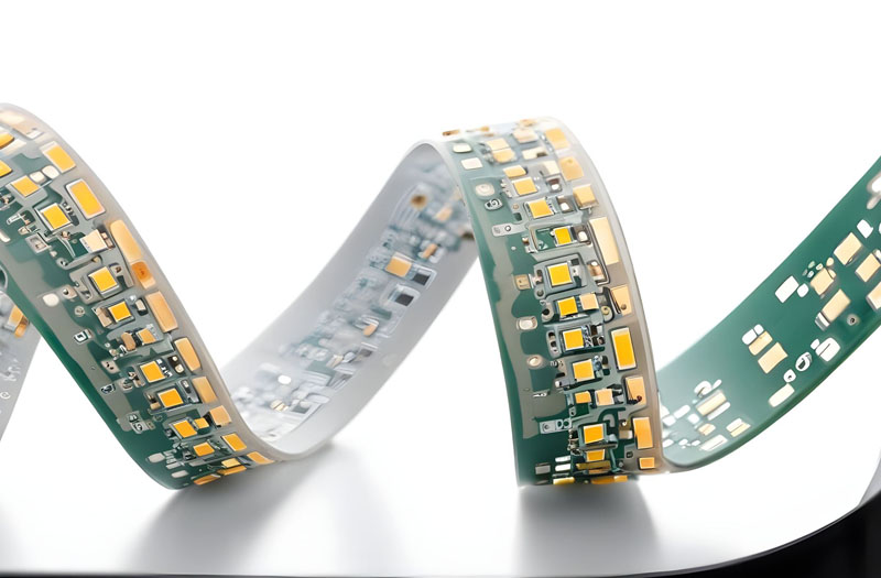
| Flex PCB | Flexible polyimide substrate | Bendable; resistant to vibration; thin profile | Wearable devices, automotive dashboards, drone cameras | Curved or movable enclosures where rigid PCBs can’t fit |
| Rigid-Flex PCB | Combination of rigid and flexible sections | Structural support + bendability; reduced assembly steps | Medical implants, satellite components, foldable phones | Complex designs needing both stability and flexibility (e.g., foldable device hinges) |
Specialty PCBs for Advanced Requirements
- High-Frequency PCB: Uses low-dielectric-loss materials like Rogers 4350B (dielectric constant: 3.48) to support frequencies ≥500MHz, resolving signal degradation in satellite communication and radar systems.
- Aluminum-Backed PCB: Dissipates 5x more heat than standard FR-4, addressing overheating in LED lighting, power supplies, and automotive engine bay electronics.
- HDI PCB (High-Density Interconnect): Features microvias (≤0.1mm) and fine-pitch traces (≤0.08mm), enabling miniaturization in portable electronics like tablets and wearables.
- Ceramic PCB: Offers exceptional thermal conductivity and chemical resistance, solving performance issues in high-temperature environments like industrial furnaces or aerospace engines.
Why PCBs Are Essential for Modern Electronics
Irreplaceable Benefits Over Traditional Wiring
- Reliability: Soldered connections and fixed component placement reduce failure rates by 80% compared to point-to-point wiring, critical for safety-critical devices like aerospace navigation systems and medical monitors.
- Space Efficiency: Multi-layer PCBs reduce device size by 60%, making it possible to create slim, portable products like laptops, wireless earbuds, and fitness trackers.
- Performance Consistency: Standardized manufacturing processes ensure uniform electrical characteristics across production runs, eliminating variability in device performance (e.g., consistent battery life in smartphones).
- Cost Savings: Automated assembly and reduced material waste lower total production costs by 40% for high-volume orders, a key advantage for consumer electronics manufacturers scaling to mass production.
- Design Flexibility: PCBs support custom layouts tailored to specific device needs, from tiny medical implants to large industrial control panels, without sacrificing performance.
Real-World Impact of PCB Technology
Without PCBs, modern electronics would face insurmountable limitations:
- Devices would be 3x larger (e.g., a smartphone would be the size of a tablet with wired connections).
- Failure rates would skyrocket (e.g., automotive sensors would fail 5x more frequently, risking safety).
- Production costs would double (e.g., printed circuit assembly would require manual wiring, increasing labor time).
- High-frequency technologies like 5G and radar couldn’t operate (wired circuits can’t maintain signal integrity at ≥24GHz).
- Miniaturization would be impossible (wearable devices like smartwatches or hearing aids wouldn’t fit on the human body).
PCB Manufacturing Process (Step-by-Step)
Core Steps in PCB Manufacturing
- Substrate Preparation: Cut FR-4 or specialty material to the target size (tolerance ±0.1mm) and clean with isopropyl alcohol to remove dust, oil, and debris.
- Copper Lamination: Bond a thin copper sheet (1oz or 2oz thickness) to the substrate using heat (180°C) and pressure (30psi) for uniform adhesion.
- Pattern Transfer: Apply a photosensitive photoresist to the copper layer, expose it to UV light through a stencil of the PCB design, and develop to reveal the trace pattern.
- Etching: Immerse the substrate in a chemical etchant (ferric chloride or ammonium persulfate) to remove unprotected copper, leaving behind the desired traces.
- Via Drilling: Use laser drilling (for microvias ≤0.15mm) or mechanical drilling (for through-holes ≥0.2mm) to create holes for interlayer connections.
- Plating: Coat vias and trace surfaces with copper (25μm thickness) via electrolytic plating to ensure electrical conductivity and corrosion resistance.
- Solder Mask Application: Apply a protective solder mask (green, black, or clear) to cover non-connection areas, curing it with UV light for durability.
- Silkscreen Printing: Add component labels, reference marks, and company logos using high-contrast ink, ensuring readability for assembly and repair.
- Final Testing: Conduct electrical continuity tests (using a flying probe tester) and automated optical inspection (AOI) to detect defects like short circuits or missing traces.
- Packaging: Seal finished PCBs in anti-static bags to protect against electrostatic discharge (ESD) during storage and shipping.
Quality Control Standards for PCB Manufacturing
- IPC-6012 specifies minimum performance requirements, including thermal shock resistance (-40°C to 125°C for 1000 cycles) and solderability (no delamination after 3x reflow cycles).
- Trace width and spacing must adhere to IPC-2221 to prevent short circuits and ensure signal integrity in high-frequency applications.
- Via void rate must be ≤0.3% to avoid signal dropout, a critical standard for 5G and radar PCBs.
- Surface finish compliance (e.g., ENIG, HASL) must meet IPC-4552 to ensure long-term reliability and compatibility with soldering processes.
PCB FAQ (Common Questions Answered)
Q: What is the difference between a PCB and a printed circuit assembly (PCA)?
A: A PCB is a bare substrate with copper traces; a PCA is a PCB with electronic components (e.g., chips, resistors) soldered onto it, forming a fully functional circuit.
Q: Which PCB material is best for high-temperature environments?
A: Aluminum-backed PCBs or ceramic substrates (e.g., alumina) are ideal—they withstand temperatures up to 250°C, unlike standard FR-4 which is limited to 130°C.
Q: How long does PCB manufacturing take?
A: Prototypes typically take 2-5 business days; mass production (10,000+ units) takes 7-14 business days, depending on complexity (e.g., layer count, material type).
Q: What is the minimum order quantity (MOQ) for PCBs?
A: Most manufacturers offer MOQs as low as 10 units for prototypes and 1000 units for mass production, with flexible options for custom PCB manufacturing projects.
Q: How do I choose the right PCB type for my project?
A: Consider component density (multi-layer for high density), operating environment (aluminum-backed for high heat), flexibility needs (flex for curved enclosures), and budget (single-layer for basic circuits).
Q: Are printing circuit boards and PCBs the same thing?
A: Yes—“printing circuit boards” is simply a longer form of the acronym “PCB,” both referring to the same substrate-based circuit technology.


![Understanding PCB Costs & Pricing [Your Complete Guide]](https://hdicircuitboard.com/wp-content/uploads/elementor/thumbs/Understanding-PCB-Costs-Pricing-Your-Complete-Guide-qzzhe6mcaxuolkux3xalfktgavumi9y1aqfbs9bpv4.webp "Understanding PCB Costs & Pricing [Your Complete Guide]")


