
What Is a PCB? Everything You Need to Know About Printed Circuit Boards
If you’ve ever wondered what powers your smartphone, medical devices, or car electronics, the answer often lies in a small but critical component: the PCB (printed circuit board). PCBs are the unsung heroes of modern technology, serving as the foundation for nearly every electronic device. But what exactly is a PCB, how does it work, and why is it so essential? This guide breaks down the basics to advanced details, addressing common pain points for hobbyists, engineers, and manufacturers alike.
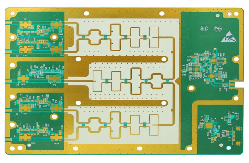
What Is a PCB? (Core Definition & Key Components)
A printed circuit board (PCB) is a structured platform that mechanically supports and electrically connects electronic components using conductive pathways—called “traces”—etched or printed onto a non-conductive base material. Unlike messy wire connections that are bulky and prone to failure, PCBs streamline component integration while ensuring reliability.
Core Components of a PCB
Every PCB, regardless of type, consists of four fundamental layers (organized from base to top):
- Substrate: The non-conductive base (often fiberglass-reinforced epoxy, known as FR-4) that provides structural rigidity. Flexible PCBs use high-temperature plastic instead, solving space constraints in tight or curved devices.
- Conductive Layer: A thin copper foil laminated to the substrate, forming the “traces” that carry electrical signals. Copper is ideal for its conductivity and affordability.
- Solder Mask: A non-conductive coating (typically green, but available in other colors) that insulates copper traces, preventing short circuits from accidental contact with solder or metal.
- Silkscreen: A white (or colored) labeling layer with text, symbols, and component markers, making assembly, troubleshooting, and repairs easier for technicians.
Common PCB Types (Solving Different Use Case Pain Points)
PCBs are not one-size-fits-all—different designs address specific challenges like space, flexibility, or complexity. Below is a breakdown of popular types:
| PCB Type | Key Features | Pain Point Solved | Typical Applications |
|---|---|---|---|
| Single-Layer PCB | 1 copper layer; simple design | Low-cost, high-volume production for basic electronics | Calculators, power supplies, simple sensors |
| Double-Layer PCB | 2 copper layers (both sides of substrate) with connecting vias | Higher component density than single-layer without excess thickness | Automotive dashboards, LED lighting, HVAC systems |
| Multilayer PCB | 3+ conductive layers separated by insulation | Complex circuitry for compact devices (reduces size/weight) | Computer motherboards, graphics cards, satellite systems |
| Flexible PCB | Bendable plastic substrate | Fitting into curved spaces or high-vibration environments | Smartphones, wearables, aerospace instrument panels |
| Rigid Flex PCB | Combination of rigid and flexible layers | Eliminating multiple PCBs in tight, dynamic devices | Pacemakers, digital cameras, car infotainment systems |
| High-Density Interconnect (HDI) PCB | Finer traces (≤100µm), smaller vias (<150µm), and higher pad density (>20 pads/cm²) | Ultra-compact designs for miniaturized electronics | Medical implants, smartphones, IoT devices |
Critical Technical Specifications to Verify
For manufacturers and designers, incorrect specs lead to costly reworks. Key parameters to confirm:
- Trace width/spacing: ≥100µm for standard PCBs; HDI PCBs use ≤100µm
- Via size: <150µm for HDI; standard vias range from 150–300µm
- Substrate material: FR-4 for most applications; Teflon for high-frequency needs
- Copper thickness: 1oz (35µm) for standard use; thick copper (2–10oz) for high-current devices (e.g., motor controllers)
Core Functions of a PCB (Why It’s Indispensable)
PCBs serve three non-negotiable roles in electronics, solving critical pain points that outdated wiring methods can’t address:
Mechanical Support for Components
Without a PCB, components like resistors, capacitors, and integrated circuits (ICs) would lack a stable mounting platform. This solves the problem of:
- Loose connections from vibrating devices (e.g., car electronics or industrial machinery)
- Component damage from physical stress (the substrate shields delicate parts)
- Disorganized layouts that make assembly/repairs impossible
Electrical Connection & Signal Routing
Traces on the PCB replace messy wires, ensuring precise, consistent signal flow. These addresses:
- Short circuits (solder mask insulates traces)
- Signal interference (layered design separates power and signal paths)
- Inefficient power distribution (optimized trace layouts reduce voltage drops)
Reliability & Durability
PCBs are manufactured to strict standards, offering long-term performance that solves:
- Frequent failures from wire corrosion or wear
- High repair costs (a defective PCB is cheaper to replace than a full device, but quality PCBs minimize this risk)
- Inconsistency in hand-wired circuits (mass-produced PCBs ensure uniformity)
How Does a PCB Work? (Step-by-Step Explanation)
Understanding PCB functionality helps troubleshoot issues and optimize designs. Here’s a simplified breakdown of how it operates, from power input to component communication:
Step 1: Power Distribution
- The PCB receives power (from a battery or external source) via a power connector.
- Copper traces route power to components like capacitors (which store charge for peak demand) and voltage regulators (which stabilize power flow).
- Pain point solved: Uneven power delivery that damages sensitive components (e.g., ICs).
Step 2: Signal Transmission
- Components like sensors or microcontrollers generate electrical signals.
- Traces act as “roads” for these signals, directing them to target components (e.g., a sensor signal sent to a microcontroller for processing).
- Vias (small holes drilled through the PCB) connect traces across layers, enabling compact designs.
- Pain point solved: Signal loss or interference in complex devices (e.g., smartphones with dozens of components).
Step 3: Component Interaction
- Key components work together to execute the device’s function:
- Resistors: Limit current flow to prevent component burnout.
- Diodes: Ensure current flows in one direction, protecting circuits from reverse voltage.
- ICs: Process signals (e.g., a CPU in a laptop or a sensor chip in a glucose monitor).
- Transistors: Amplify or switch signals, enabling functions like volume control in speakers.
- Pain point solved: Uncoordinated component behavior that renders the device useless.
Step 4: Heat Management
- High-power components (e.g., LED drivers, motor controllers) generate heat.
- Substrates like FR-4 or aluminum-backed PCBs dissipate heat, preventing overheating.
- Aluminum-backed PCBs are ideal for high-heat applications, solving the problem of component failure due to thermal stress.
Where Are PCBs Used? (Real-World Applications)
PCBs are ubiquitous across industries, with specialized designs tailored to sector-specific pain points. Below are key use cases:
Consumer Electronics
- Devices: Smartphones, laptops, smartwatches, TVs, and gaming consoles.
- PCB Type: HDI, flexible, and rigid flex PCBs.
- Pain Point Solved: Miniaturization (HDI PCBs pack more components into small spaces) and durability (flexible PCBs withstand daily wear, like bending in foldable phones).
Medical Devices
- Devices: Pacemakers, blood glucose monitors, X-ray machines, and CAT scanners.
- PCB Type: HDI, flexible, and rigid PCBs.
- Pain Point Solved: Small size (critical for implants), sterility (PCB materials are non-toxic), and reliability (failure-free operation in life-saving devices).
Automotive & Aerospace
- Devices: Car infotainment systems, engine controllers, aircraft navigation systems.
- PCB Type: Flexible, rigid flex, and thick copper PCBs.
- Pain Point Solved: High vibration resistance (flexible PCBs don’t crack) and weight reduction (rigid flex PCBs replace multiple boards, cutting vehicle/aerospace weight).
Industrial Machinery
- Devices: Motor controllers, high-current chargers, load testers.
- PCB Type: Thick copper and rigid PCBs.
- Pain Point Solved: High-current handling (thick copper traces prevent overheating) and durability in harsh factory environments.
Lighting
- Devices: LED bulbs, traffic lights, industrial lighting.
- PCB Type: Aluminum-backed PCBs.
- Pain Point Solved: Heat dissipation (aluminum transfers heat away from LEDs, extending lifespan and preventing dimming).
FAQ: Common PCB Questions (Answering User Pain Points)
Q1: How do I choose the right PCB type for my project?
A: Start with three key factors: 1) Space constraints (use flexible/rigid flex for tight/curved areas), 2) Complexity (multilayer/HDI for dense components), and 3) Environment (thick copper for high current, aluminum-backed for heat). For beginners, single-layer PCBs are ideal for simple projects like Arduino shields.
Q2: What’s the difference between a PCB and a PCB prototype?
A: A PCB prototype is a small-batch version of the final design, used to test functionality before mass production. It solves the pain point of costly reworks—catching design flaws early saves time and money.
Q3: Why do PCBs fail, and how can I prevent it?
A: Common failures include trace corrosion (solve with high-quality solder mask), overheating (use appropriate substrate/copper thickness), and poor soldering (work with ISO-certified manufacturers). For high-reliability applications (e.g., medical devices), choose PCBs tested to IPC standards.
Q4: Are flexible PCBs more expensive than rigid ones?
A: Yes, due to specialized materials and manufacturing processes. However, they often reduce overall costs by replacing multiple rigid PCBs, cutting assembly time and weight.
Q5: What is high-density interconnect (HDI) PCB, and when do I need it?
A: HDI PCBs have finer traces, smaller vias, and higher component density. Use them for miniaturized devices like smartphones, wearables, or medical implants where space is critical.
Key Takeaways for PCB Success
- Choose the right type: Match PCB design to your project’s space, complexity, and environment needs.
- Prioritize quality: Defective PCBs lead to costly device failures—work with manufacturers that follow IPC standards and offer prototyping.
- Leverage prototypes: Test PCB designs early to fix flaws before mass production.
- Focus on specs: Verify trace width, via size, and substrate material to avoid performance issues.
PCBs are the backbone of modern electronics, and understanding their design, function, and applications is critical for anyone working with electronics—from hobbyists to industry professionals. By addressing common pain points like space constraints, reliability, and cost, the right PCB design ensures your device performs as intended, every time.


![Understanding PCB Costs & Pricing [Your Complete Guide]](https://hdicircuitboard.com/wp-content/uploads/elementor/thumbs/Understanding-PCB-Costs-Pricing-Your-Complete-Guide-qzzhe6mcaxuolkux3xalfktgavumi9y1aqfbs9bpv4.webp "Understanding PCB Costs & Pricing [Your Complete Guide]")


