
Introduction to Printed Circuit Board (PCB) in Electronics
Printed Circuit Boards (PCBs) are the fundamental building blocks of modern electronics manufacturing, serving as the structural and electrical backbone for devices spanning consumer gadgets to industrial systems. These boards replace disorganized wiring with precise, insulated pathways, enabling compact, reliable, and scalable electronic designs. From flexible pcb for wearable tech to high density interconnect (HDI) PCBs for advanced computing, PCBs adapt to diverse application needs, making them indispensable in electronics manufacturing.
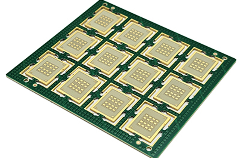
What Is PCB?
Core Definition of a PCB
A Printed Circuit Board (PCB) is a flat structure crafted from non-conductive substrate materials—commonly fiberglass (FR-4) or composite epoxy—with conductive copper traces etched or printed onto its surface. These traces act as dedicated pathways for electrical signals, facilitating communication between electronic components. A bare PCB lacks functional components and serves solely as a platform, requiring assembly to deliver operational value. This foundational role makes PCBs the starting point for all electronic devices, from simple toys to complex aerospace systems.
Key Components of a PCB
Every PCB integrates essential elements that ensure electrical connectivity, structural integrity, and usability, each designed to address specific manufacturing and operational requirements:
- Traces: Thin copper pathways that transmit electrical signals; width and spacing follow IPC-2221 standards (minimum 0.008” width for 1oz copper) to support current flow and prevent signal interference.
- Pads: Exposed copper regions where components are soldered, providing secure mechanical and electrical connections.
- Vias: Plated holes that connect traces across multiple layers, critical for multi-layer and HDI PCB designs to save space.
- Silkscreen: Printed markings (component labels, reference designators) that streamline assembly, testing, and maintenance.
- Solder Mask: A protective polymer layer (typically green) that covers non-essential copper areas, preventing short circuits and corrosion.
- Substrate: The base material (e.g., FR-4, polyimide for flexible pcb) that provides insulation and mechanical support.
PCB Types: Detailed Comparison and Selection
Choosing the right PCB type is critical for meeting application constraints, with variations tailored to form factor, complexity, and environment. Below is a detailed comparison of key types, including pcb prototype, flexible pcb, rigid flex pcb, and high density interconnect (HDI) PCB:
| PCB Type | Structure & Materials | Core Features | Typical Applications | Electronics Manufacturing Considerations |
|---|---|---|---|---|
| Single-Layer PCB | One conductive copper layer on a rigid substrate (FR-4) | Low cost, simple design, easy fabrication | Calculators, remote controls, basic sensors | Ideal for low-complexity, high-volume production; limited component density |
| Double-Layer PCB | Two conductive layers separated by substrate, connected via vias | Moderate component density, balanced cost-performance | Power supplies, audio equipment, industrial controllers | Complies with IPC-6012 Type 2; suitable for mid-range complexity |
| Multi-Layer PCB | 4–40+ conductive layers with insulating substrate layers | High component density, improved signal integrity | Smartphones, servers, medical devices | Requires precise lamination; adheres to IPC-6012 Type 3 for high-reliability applications |
| Flexible PCB | Thin, bendable substrate (polyimide) with copper traces | Conforms to tight spaces, vibration-resistant | Wearables, automotive wiring harnesses, foldable devices | Resists temperature extremes (-40°C to 120°C); lighter than rigid alternatives |
| Rigid Flex PCB | Combination of rigid FR-4 sections and flexible polyimide segments | Combines rigidity for components with flexibility for routing | Aerospace systems, robotic arms, portable medical devices | Reduces assembly steps by 30% vs. separate rigid/flex boards; requires specialized tooling |
| High Density Interconnect (HDI) PCB | Microvias (≤0.15mm), fine-pitch traces (≤0.1mm), stacked layers | Ultra-high component density, faster signal transmission | 5G devices, laptops, advanced semiconductors | Uses laser drilling; complies with IPC-2226 standards for microvia design |
| PCB Prototype | Small-batch (1–100 units) production of any PCB type | Rapid turnaround (2–5 days), design validation | New product development, testing, market trials |
PCB Function: Core Roles in Electronics
PCBs perform four critical functions that underpin the operation of electronic devices, addressing key challenges in signal transmission, component integration, and reliability:
Signal Routing and Transmission
- Copper traces act as “electrical highways” that direct power and data signals between components, minimizing signal loss and interference.
- High density interconnect (HDI) PCBs use microvias and fine traces to support high-speed signals (up to 10 Gbps) in compact designs, ideal for 5G and data center applications.
- Adherence to IPC-2221 impedance standards ensures signal integrity, preventing distortion in sensitive electronics like medical monitors.
Component Support and Integration
- Provides a stable platform for mounting resistors, capacitors, integrated circuits (ICs), and other components, eliminating loose wiring and reducing assembly errors.
- Rigid flex pcb enables integration of components in complex geometries (e.g., curved surfaces in automotive dashboards) without compromising connectivity.
- PCB prototype allows for testing component placement and compatibility before full-scale electronics manufacturing, reducing rework costs.
Thermal Management
- Copper traces and ground planes dissipate heat generated by high-power components, preventing overheating and extending device lifespan.
- Flexible pcb uses thermally conductive polyimide substrates that handle temperature fluctuations, making them suitable for under-hood automotive applications.
- Multi-layer HDI PCBs incorporate thermal vias to transfer heat from internal layers to the surface, improving efficiency by 25% in high-performance devices.
Reliability and Durability
- Eliminates short circuits and connection failures caused by vibration or environmental factors, critical for aerospace and industrial electronics.
- Rigid flex pcb reduces the number of connectors by 40% vs. traditional wiring, lowering failure points in mission-critical systems.
- Compliance with IPC-6012 quality standards ensures consistent performance across temperature ranges (-55°C to 125°C) and humidity levels.
PCB Examples: Real-World Applications Across Industries
PCBs are ubiquitous in electronics, with specialized types addressing industry-specific needs. Below are practical examples that highlight the versatility of PCB, flexible pcb, rigid flex pcb, and HDI PCB:
Consumer Electronics
- Smartphones: Multi-layer HDI PCBs with microvias (0.1mm diameter) and stacked layers, supporting processors, cameras, and 5G modems in compact form factors.
- Wearable Devices: Flexible pcb made from polyimide, conforming to wristbands and fitness trackers while withstanding bending and sweat exposure.
- Laptops: Rigid flex pcb connecting motherboards to displays and batteries, reducing weight by 15% compared to traditional wiring.
- Home Appliances: Single-layer PCBs in refrigerators and ovens, controlling temperature sensors and power distribution with cost-effective design.
Industrial and Automotive
- Industrial Controllers: Multi-layer PCBs adhering to IPC-6012 Type 3, operating reliably in factory environments with temperature swings and electrical noise.
- Automotive ADAS: Rigid flex pcb integrated into advanced driver-assistance systems, routing signals between cameras, radar, and control units while resisting vibration.
- Electric Vehicles: High density interconnect (HDI) PCBs in battery management systems, monitoring cell voltage and temperature with precision.
Medical Devices
- Implantable Devices: Flexible pcb with biocompatible materials, used in pacemakers and neurostimulators to conform to body contours.
- Diagnostic Equipment: HDI PCBs in MRI machines and blood analyzers, supporting high-speed data processing and sensitive sensors.
- Portable Monitors: PCB prototypes tested for durability and accuracy before mass production, ensuring compliance with medical device regulations.
Aerospace and Defense
- Satellite Systems: Rigid flex pcb that withstands radiation and extreme temperatures (-65°C to 150°C) while reducing launch weight.
- Radar Systems: High density interconnect (HDI) PCBs with ultra-fine traces, enabling precise signal processing for defense applications.
- Unmanned Aerial Vehicles (UAVs): Lightweight flexible pcb that fits into tight spaces without compromising structural integrity.
PCBA: From Bare PCB to Functional Assembly
What Is a PCBA?
A Printed Circuit Board Assembly (PCBA) is a bare PCB that has been populated with electronic components (resistors, capacitors, ICs, connectors) through soldering. Unlike a bare PCB, a PCBA is a fully functional unit ready for integration into final products. The assembly process leverages two primary technologies, each suited to different component types and production volumes:
- Surface Mount Technology (SMT): Components are mounted directly onto the PCB’s surface using solder paste and reflow soldering, ideal for miniaturized parts and high-volume electronics manufacturing.
- Through-Hole Technology: Components are inserted into pre-drilled holes and soldered on the opposite side, offering enhanced mechanical stability for larger, heavier components.
PCB vs. PCBA: Key Differences
| Feature | PCB | PCBA |
|---|---|---|
| Definition | Bare board with copper traces and substrate (no components) | Populated PCB with soldered components |
| Function | Provides a platform for component mounting | Delivers full electronic functionality |
| Manufacturing Stages | Fabrication (etching, drilling, lamination) | Fabrication + component placement + soldering + testing |
| Usability | Cannot perform electronic tasks independently | Ready for integration into end products |
| Cost | Lower (material and fabrication only) | Higher (includes components and assembly) |
PCB vs. PCA: Clarifying Terminology
A common point of confusion is the difference between PCB and PCA (Printed Circuit Assembly). PCA is simply an alternative term for PCBA—both refer to an assembled PCB with functional components. The key distinction remains between the bare PCB (unpopulated) and the PCA/PCBA (populated, functional). This terminology overlap is important in electronics manufacturing, as it ensures clear communication between designers, manufacturers, and buyers.
PCB Manufacturing and Prototyping
PCB Manufacturing Process
The production of PCBs—from design to finished board—involves structured steps that adhere to industry standards (IPC-6012, IPC-2221) to ensure quality:
- Design: Create schematics and layout files using CAD software, optimizing for trace width, via placement, and component density.
- Fabrication:
- Substrate cutting: Trim raw substrate (FR-4, polyimide for flexible pcb) to desired dimensions.
- Copper lamination: Apply copper foil to substrate layers using heat and pressure.
- Etching: Use photoresist and acid to remove excess copper, leaving precise traces.
- Drilling: Create holes for vias and component leads (laser drilling for HDI PCB microvias).
- Plating: Coat holes with conductive material (gold, tin) to ensure connectivity.
- Solder mask and silkscreen application: Add protective layer and labeling.
- Testing: Conduct automated optical inspection (AOI), in-circuit testing (ICT), and functional testing to detect defects.
PCB Prototype: Purpose and Benefits
PCB prototype is a small-batch production run (1–100 units) that serves as a test version of the final PCB. Key advantages include:
- Validating design functionality before high-volume manufacturing, reducing the risk of costly revisions.
- Testing component compatibility and performance in real-world conditions.
- Enabling rapid iterations (2–5 day turnaround) to address design flaws.
- Supporting customization for niche applications (e.g., specialized flexible pcb for medical devices).
FAQ: Common PCB Questions
How do I choose the right PCB type for my project?
Consider application requirements: use flexible pcb for bendable designs, rigid flex pcb for mixed-form-factor needs, HDI PCB for high-density components, and PCB prototype for testing. Factor in complexity, environment (temperature, vibration), and production volume.
What are the key standards for PCB manufacturing?
IPC-2221 (design standards for printed boards) and IPC-6012 (performance specifications for rigid PCBs) are the most widely adopted. IPC-2226 specifically governs HDI PCB design, while IPC-2223 covers flexible pcb requirements.
How long does PCB prototype production take?
Typical turnaround time is 2–5 business days for standard prototypes; expedited services can deliver in 1–2 days. Complex designs (e.g., HDI PCB, rigid flex pcb) may take 5–7 days.
What is the difference between flexible pcb and rigid flex pcb?
Flexible pcb is fully bendable, while rigid flex pcb combines rigid sections (for component mounting) with flexible segments (for routing). Rigid flex pcb is ideal for applications requiring both stability and flexibility.
Conclusion
Printed Circuit Boards (PCBs) are the backbone of modern electronics, with diverse types—from flexible pcb to high density interconnect (HDI) PCB—addressing the unique needs of every industry. Understanding what a PCB is, its functions, examples, and how it evolves into a PCBA is essential for successful electronics manufacturing. Whether selecting a PCB prototype for testing or a rigid flex pcb for aerospace applications, adherence to industry standards (IPC-2221, IPC-6012) and careful type selection ensure optimal performance, reliability, and cost-effectiveness. As technology advances, PCBs will continue to enable innovation, powering the next generation of electronic devices.


![Understanding PCB Costs & Pricing [Your Complete Guide]](https://hdicircuitboard.com/wp-content/uploads/elementor/thumbs/Understanding-PCB-Costs-Pricing-Your-Complete-Guide-qzzhe6mcaxuolkux3xalfktgavumi9y1aqfbs9bpv4.webp "Understanding PCB Costs & Pricing [Your Complete Guide]")


