Core Definition of PCB Board
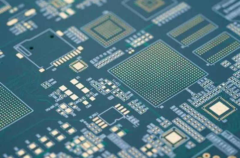
A PCB (printed circuit board) is a flat, structured platform that mechanically supports and electrically connects electronic components using conductive pathways etched onto non-conductive substrates. Serving as the backbone of modern electronics, PCB boards replace traditional point-to-point wiring, enabling compact, reliable, and high-performance device designs. From smartphones and laptops to industrial machinery and medical equipment, every electronic device with an on-switch relies on a PCB or its assembled form, the PCBA (printed circuit board assembly).
Base Material: The Foundation of PCB Boards
Common Base Materials
- FR4: Fiberglass-reinforced epoxy resin, the most widely used base material for rigid PCBs due to its balance of cost, durability, and thermal stability
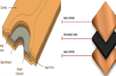
- Polyimide (PI): Flexible, high-temperature-resistant material ideal for flexible pcb and rigid flex pcb applications
- Metal-core: Aluminum or copper substrates used for rf pcb and high-power circuits, offering enhanced heat dissipation
- Ceramic: Used in high-frequency or high-temperature applications, providing excellent electrical insulation and thermal conductivity
- Epoxy-phenolic: Low-cost alternative for basic single-sided PCBs, common in low-end consumer electronics
Material Selection Criteria
- Mechanical strength: Rigidity for stationary devices (FR4) vs. flexibility for wearables (polyimide)
- Thermal performance: Critical for high-power circuits (metal-core) to prevent overheating
- Electrical properties: Insulation resistance and signal integrity, especially for hdi pcb and rf pcb
- Cost: Balancing performance needs with budget constraints (FR4 for cost-effectiveness, ceramic for specialized use)
- Compliance: RoHS and IPC-2221 standards for material safety and performance
Layers: Structure of PCB Boards
Basic Layer Composition
- Substrate: Core non-conductive layer (e.g., FR4, polyimide) providing mechanical support
- Copper layer: Thin foil (typically 1–3 oz/sq ft) forming conductive pathways; thickness varies by current requirements
- Soldermask: Insulative layer (commonly green, but available in red, black, or white) protecting copper traces from short circuits and corrosion
- Silkscreen: Top layer with printed labels, symbols, and component identifiers for assembly and maintenance
Layer Configuration Variations
- Single-layer: Copper on one side of the substrate; simplest and most cost-effective design
- Double-layer: Copper on both sides, connected via plated through-holes (PTH)
- Multi-layer: Three or more copper layers separated by insulating substrates; up to 40+ layers for complex applications
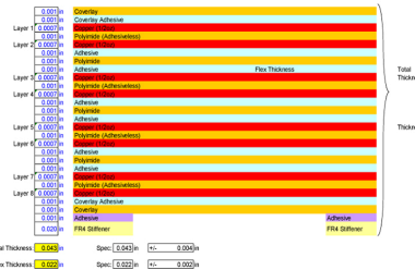
- Rigid flex pcb: Combination of rigid (FR4) and flexible (polyimide) layers for 3D packaging and space-constrained designs
Traces: Conductive Pathways of PCB Boards
Trace Characteristics
- Material: Primarily copper, chosen for high conductivity and cost-effectiveness
- Dimensions: Width ranges from 0.003″ (76 µm) to 0.2″ (5 mm); thickness corresponds to copper weight (1 oz = 35 µm)
- Function: Transmit electrical signals and power between components with minimal resistance
- Design Rules: Compliant with IPC-2221 standards, specifying minimum trace width (based on current) and spacing (to prevent crosstalk)
Trace Optimization for Performance
- Width adjustment: Thicker traces (2–3 oz copper) for high-current applications (e.g., power supplies)
- Routing techniques: Short, direct paths to reduce signal delay; ground planes to minimize interference
- Impedance control: Critical for rf pcb and high-speed circuits, ensuring consistent signal transmission
Components: Active & Passive Elements on PCB Boards
Active Components
- Transistors: Act as switches or amplifiers, controlling current flow in digital and analog circuits
- Diodes: Regulate current direction, protecting components from reverse voltage
- Integrated Circuits (ICs): Microcontrollers, memory chips, and processors that serve as the “brain” of the device
- Sensors: Detect environmental conditions (temperature, pressure) and convert to electrical signals
- Amplifiers: Boost weak signals for communication or processing
Passive Components
- Resistors: Regulate current flow and voltage levels; color-coded for value identification
- Capacitors: Store electrical charge, filtering noise and stabilizing power supplies
- Inductors: Store energy in magnetic fields, used in filtering and power conversion
- Transformers: Step up or step down voltage for compatibility with components
- Relays: Electromechanical switches controlling high-power circuits with low-power signals
Vias: Interlayer Connections in PCB Boards
Via Types and Applications
| Via Type | Definition | Common Uses |
|---|---|---|
| Through-hole Via | Passes through all layers of the PCB | Double-layer and multi-layer PCBs; general-purpose connections |
| Blind Via | Connects outer layer to inner layers without penetrating the entire board | Multilayer PCB and HDI PCB; saves space and reduces crosstalk |
| Buried Via | Connects inner layers only, hidden from outer surfaces | High-density interconnect (HDI) designs; complex multi-layer PCBs |
| Microvia | Small-diameter via (<150 µm) per IPC-2226 standards | HDI PCB and HDI circuit boards; miniaturized electronics (smartphones, wearables) |
Via Design Considerations
- Size: Microvias enable higher component density in hdi pcb, reducing board footprint by up to 30%
- Placement: Strategic routing to avoid trace interference; compliance with minimum spacing rules
- Plating: Copper-plated walls ensuring reliable electrical connection between layers
- Tenting: Soldermask coverage for protection against solder bridges and environmental damage
Core Functions of PCB Boards
Connects Components
- Establishes reliable electrical connections between discrete components (resistors, capacitors) and integrated circuits
- Eliminates loose wires, reducing assembly errors and failure rates compared to point-to-point wiring
- Supports both through-hole technology (THT) and surface-mount technology (SMT) components for versatile design
Routes Signals
- Directs data and power signals along optimized paths, minimizing signal loss and delay
- Implements ground planes and shielding to reduce electromagnetic interference (EMI)
- Enables differential signaling for high-speed data transfer in hdi pcb and rf pcb
Provides Support
- Mechanically secures components, preventing damage from vibration and environmental stress
- Maintains component alignment for consistent performance and ease of assembly
- Offers structural integrity for device packaging and handling
Reduces Noise
- Compact component placement minimizes parasitic capacitance and inductance, reducing electrical noise
- Ground pours and decoupling capacitors stabilize voltage, filtering out unwanted signals
- Controlled impedance traces in rf pcb prevent signal reflections and crosstalk
PCB Board Types: Single-sided, Double-sided & Multi-layer
Single-sided PCB
- Structure: Copper traces on one side of the substrate; components mounted on the same side
- Key Features: Low cost, simple design, easy manufacturing; limited component density
- Applications: Calculators, radios, LED lights, basic sensors; ideal for low-complexity devices
- Limitations: Cannot support complex circuits; trace crossing requires jumpers
Double-sided PCB
- Structure: Copper on both sides, connected via plated through-holes; components on one or both sides
- Key Features: Higher component density than single-sided; versatile for medium-complexity designs
- Applications: Mobile phones, printers, routers, modems; balances performance and cost
- Advantages: Reduced board size; supports mixed THT and SMT components
Multi-layer PCB
- Structure: Three or more copper layers (typically 4–16 layers, up to 40+); inner layers for power and ground
- Key Features: Maximum component density; excellent signal integrity; supports high-speed and high-power circuits
- Applications: Computers, servers, medical equipment (MRI machines), aerospace systems; complex electronics
- Variations: Hdi pcb with microvias and high connection density (>20 pads/cm²) per IPC-2226
Specialized PCB Types
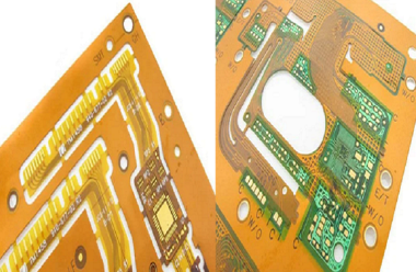
- Flexible pcb (flexible printed circuit): Polyimide substrate for bendable, lightweight designs; used in wearables and foldable devices
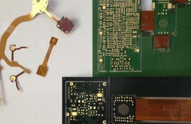
- Rigid flex pcb: Combines rigid and flexible layers; ideal for 3D packaging in aerospace and medical devices
- Rf pcb: Optimized for radio frequency signals; used in communication equipment and antennas
- High density interconnect (HDI) pcb: Fine lines (<100 µm), microvias, and dense pads; enables miniaturization in smartphones and IoT devices
FAQ: Common Questions About PCB Boards
What is the difference between PCB and PCBA?
- PCB: Bare board with substrate, copper traces, soldermask, and silkscreen; no mounted components
- PCBA: Assembled PCB with soldered components (resistors, ICs, sensors); fully functional electronic assembly
How to choose the right PCB type for a project?
- Single-sided: Low-cost, simple circuits (e.g., LED flashlights)
- Double-sided: Medium-complexity devices (e.g., home routers)
- Multi-layer: High-performance electronics (e.g., laptop motherboards)
- Flexible pcb: Wearables or bendable designs (e.g., smartwatch straps)
- Hdi pcb: Miniaturized, high-density devices (e.g., smartphones)
What are the key standards for PCB manufacturing?
- IPC-2221: Governs PCB design requirements (trace width, spacing, material selection)
- IPC-6012: Specifies performance standards for rigid PCBs
- IPC-2226: Defines requirements for high density interconnect (HDI) pcb
- RoHS: Restricts hazardous substances in PCB materials and manufacturing
How do vias impact PCB performance?
- Microvias in hdi pcb reduce signal path length, improving speed and reducing crosstalk
- Blind and buried vias save board space, enabling smaller, more compact designs
- Proper via placement prevents signal reflections and ensures reliable interlayer connections
What materials are used for flexible pcb?
- Polyimide (PI) substrate: Offers flexibility, heat resistance, and durability
- Copper traces: Thin foil (1 oz) for flexibility without compromising conductivity
- Adhesive layers: Bond copper to substrate; chosen for flexibility and thermal stability
Evolution and Future of PCB Boards
PCB technology has evolved from simple single-sided designs to complex multilayer pcb and hdi circuit boards, driven by the demand for smaller, more powerful electronics. Future innovations include:
- Transparent PCBs using glass or ceramic substrates for next-gen displays
- Stretchable PCBs for wearable and implantable medical devices
- Enhanced thermal management materials for high-power applications
- Integration of sensors and antennas directly into the PCB structure
- Advancements in hdi pcb with even finer lines and microvias, supporting 5G and IoT technologies
As electronics continue to miniaturize and demand higher performance, PCB boards remain critical to innovation across industries—from consumer gadgets to aerospace and healthcare. Understanding their structure, materials, and types empowers designers and manufacturers to create reliable, efficient, and cutting-edge electronic products.

![Understanding PCB Costs & Pricing [Your Complete Guide] Understanding PCB Costs & Pricing [Your Complete Guide]](https://hdicircuitboard.com/wp-content/uploads/elementor/thumbs/Understanding-PCB-Costs-Pricing-Your-Complete-Guide-qzzhe6mcaxuolkux3xalfktgavumi9y1aqfbs9bpv4.webp)
