
How to Make a Circuit Board? Complete Guide to PCB Prototype & Manufacturing
Design: Lay the Foundation for Functional PCB Prototypes
Design Software Selection
- KiCad: Open-source, free, compatible with Windows, macOS, Linux; sufficient for hobbyists and commercial projects
- EasyEDA: Cloud-based online tool with intuitive interface, ideal for beginners’ first printed circuit board prototype
- Eagle CAD: Widely used for schematic design and PCB layout, extensive component library access
- Diptrace: CAD software with four modules (Schematic Capture, PCB Layout, Component Editor, Pattern Editor); supports complex designs
- Altium Designer: Professional-grade tool for advanced projects, available as a time-limited demo
PCB Design Process
- Create a detailed circuit schematic outlining all components (resistors, capacitors, LEDs) and connections
- Verify component footprints and pinouts using existing libraries to avoid manual entry errors
- Design PCB layout with 2-layer configuration for most basic to mid-range projects
- Implement ground pour to reduce noise and improve signal integrity
- Mark polarity and component functions on the silkscreen for accurate assembly
- Validate schematic-to-footprint alignment through multiple checks to prevent non-functional boards
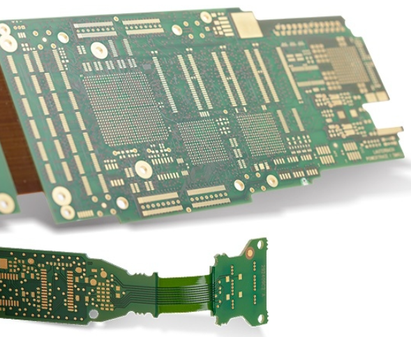
Flexible PCB Design Considerations
- Use flexible substrates (e.g., Kapton-based materials) for flexible printed circuit projects
- Ensure trace widths and spacing comply with IPC-2221 standards for flexible circuits
- Avoid sharp angles in traces to maintain flexibility and prevent cracking
- Design for proper heat dissipation during soldering to protect flexible materials
DIY Home Etching Method: Build PCB Prototypes at Home
Materials Required
- Copper-coated circuit board (standard size: 3.5×5 inches; flexible option: copper tape + Kapton tape)
- Etchant (ferric chloride or ammonium persulfate, compliant with safety standards)
- Glossy paper/magazine paper/photo paper for design transfer
- Laser printer or photocopying machine (inkjet printers incompatible due to water-soluble ink)
- Flat iron (for toner transfer)
- Plastic container (non-corrosive, for etching)
- Plastic tweezers (for handling circuit boards during etching)
- Mini drill/Dremel with 0.8-1mm high-speed steel or carbide drill bits
- Safety goggles, gloves, protective mask (for chemical and dust protection)
- Sanding paper (1200 grit for cleaning and finishing)
- Acetone-free nail polish remover (for cleaning residual ink)
- Ruler, scouring pad, microfiber towel
Transfer: Apply Design to Copper Board
- Print the PCB layout in reverse on glossy paper using a laser printer
- Clean the copper board surface with acetone to remove oils and debris
- Position the printed design face-down on the copper surface, ensuring full contact
- Heat the iron to medium-high (180-220°C) and apply firm pressure for 45 seconds to 3 minutes
- Submerge the board in water for 2-5 minutes to soften the paper
- Gently rub off the paper to reveal the transferred ink pattern on the copper
Etch: Remove Unwanted Copper
- Pour etchant into a plastic container in a well-ventilated area
- Warm ferric chloride to 46°C (max) to accelerate etching without toxic fume release
- Place the circuit board face-down on plastic risers in the etchant
- Agitate the container periodically with plastic tweezers for uniform etching
- Etch for 5-45 minutes (varies by board size and etchant type) until non-protected copper is fully removed
- Rinse the PCB thoroughly with running water to stop the etching process
Drill & Solder: Finalize DIY PCB Assembly
- Mark component mounting positions using a PCB push hand drill for precision
- Drill 0.03-inch (0.8mm) holes for through-hole components; skip drilling for SMDs
- Wear a protective mask to avoid inhaling toxic copper dust during drilling
- Sand the board edges with fine-grit sandpaper to smooth surfaces
- Remove residual ink with sanding paper or acetone-free nail polish remover
- Position components according to polarity markings on the silkscreen
- Solder components using a soldering iron, ensuring secure connections compliant with IPC-A-610 standards
- Test the circuit with a multimeter to verify connectivity and functionality
Professional Manufacturing: High-Quality PCB Production
Generate Manufacturing Files
- Export Gerber files (inclusive of copper layers, silkscreen, solder mask, drill data)
- Create NC drill files specifying hole sizes and locations
- Verify file compatibility with manufacturer requirements (e.g., Gerber RS-274X format)
- Compress files into a single ZIP folder for upload
Order Process
- Select a professional electronics manufacturing service specializing in PCB prototype production
- Upload Gerber and NC drill files through the manufacturer’s platform
- Specify PCB parameters: layer count (2-layer to multi-layer), substrate material (FR-4, flexible Kapton), thickness (1.6mm standard), solder mask color
- Choose quantity (1-100+ units) based on project needs
- Confirm lead time and shipping details
- Approve manufacturer’s design review (when provided) before production
Professional PCB Assembly
- Manufacturers use automated pick-and-place machines for precise component placement
- Reflow soldering (for SMDs) or wave soldering (for through-hole components) ensures consistent joints
- Compliance with IPC-6012 standards for PCB quality and IPC-A-610 for assembly
- Post-assembly testing includes visual inspection, X-ray inspection (for BGA components), and functional testing
- Final cleaning removes flux residues and contaminants
Steps & Tools: Detailed Breakdown for PCB Production
Step-by-Step Comparison: DIY vs. Professional Manufacturing
| Step | DIY Home Etching | Professional Manufacturing |
|---|---|---|
| Design | Manual verification of footprints | Automated DFM (Design for Manufacturing) checks |
| Transfer | Toner transfer with iron | Industrial lithography or laser ablation |
| Etching | Chemical etchant (ferric chloride) | Acid etching or plasma etching |
| Drilling | Manual mini drill | CNC drilling machines with high precision |
| Soldering | Handheld soldering iron | Automated soldering systems |
| Lead Time | 1-2 days (excluding design) | 3-10 days (varies by quantity) |
| Cost (per unit) | $5-$20 (materials) | $2-$50 (scales with quantity) |
| Quality | Suitable for prototypes | Compliant with IPC standards for mass production |
Essential Tools for Every PCB Project
- Design: Computer with PCB design software (KiCad, EasyEDA)
- Transfer: Laser printer, glossy paper, flat iron
- Etching: Plastic container, etchant, plastic tweezers
- Drilling: Mini drill/Dremel, carbide drill bits (0.8-1mm)
- Soldering: Soldering iron, solder wire (60/40 tin-lead or lead-free), desoldering gun
- Testing: Multimeter, continuity tester
- Flexible PCB: Copper tape, Kapton tape, transparent sheet (200 microns)
Safety: Compliance & Protection for PCB Manufacturing
- Wear chemical-resistant gloves, safety goggles, and old clothing when handling etchants
- Use a well-ventilated workspace during etching to avoid inhaling toxic fumes
- Store etchants in non-corrosive, sealed containers; never use metal containers
- Dispose of used etchant according to local environmental regulations (do not pour down metal pipes)
- Wear a dust mask during drilling to prevent copper dust inhalation
- Keep fire extinguishers nearby when soldering; avoid soldering near flammable materials
- Ensure proper ventilation during soldering to reduce exposure to flux fumes
FAQ: Common Questions About PCB Production
What is the difference between PCB and PCA?
- PCB (Printed Circuit Board): Bare board with conductive tracks on a non-conductive substrate
- PCA (Printed Circuit Assembly): PCB with mounted and soldered components (completed assembly)
How to choose between rigid and flexible PCB?
- Rigid PCB: Ideal for stationary electronics (e.g., Arduino projects, consumer devices); uses FR-4 substrate
- Flexible PCB: Suitable for compact, movable designs (e.g., wearables, medical devices); uses Kapton or similar flexible materials
Can I make a PCB without soldering?
- Yes, simple circuits use tape, clips, or connectors for component attachment; soldering required for durable, high-performance PCB assembly
What IPC standards apply to PCB manufacturing?
- IPC-2221: Specifies design requirements for printed circuit boards
- IPC-6012: Defines performance specifications for rigid PCBs
- IPC-A-610: Establishes acceptability criteria for electronic assemblies
How to resolve common PCB issues?
- Non-functional board: Verify schematic-to-footprint alignment and component polarity
- Poor trace adhesion: Ensure proper cleaning of copper surface before design transfer
- Etching inconsistencies: Agitate the board periodically and maintain etchant temperature within recommended range
- Solder bridges: Use flux and precise soldering technique; clean excess solder with a desoldering gun
Electronics Manufacturing Services: Scaling From Prototype to Production
- PCB prototype production: Low-quantity (1-10 units) manufacturing for design validation
- Volume production: Automated assembly lines for 100+ units, reducing per-unit cost
- Turnkey services: End-to-end solutions including design, manufacturing, assembly, and testing
- Compliance support: Adherence to industry standards (IPC, RoHS) for global market access
- Flexible printed circuit manufacturing: Specialized processes for bendable, compact designs
This guide covers the full spectrum of PCB manufacturing, from DIY home etching for printed circuit board prototypes to professional electronics manufacturing services for mass production. By following industry standards and using the right tools, anyone can create functional PCBs, flexible printed circuits, and complete PCB assemblies tailored to their project needs.


![Understanding PCB Costs & Pricing [Your Complete Guide]](https://hdicircuitboard.com/wp-content/uploads/elementor/thumbs/Understanding-PCB-Costs-Pricing-Your-Complete-Guide-qzzhe6mcaxuolkux3xalfktgavumi9y1aqfbs9bpv4.webp "Understanding PCB Costs & Pricing [Your Complete Guide]")


