
How to Make PCB: Step-by-Step Guide for DIY and Professional Circuit Board Production
Making a high-quality PCB or circuit board requires precise adherence to structured workflows, whether for small-batch DIY PCB projects or large-scale professional PCB manufacturing. The process spans from initial Design to final Testing & Finishing, with critical milestones that directly impact performance—especially for specialized boards like rigid flex pcb, pcb flex rigid, flexible pcb, flexible printed circuit, rf pcb, rf circuit board, multilayer pcb, microvia-integrated boards and high density interconnect HDI PCB. Skipping key steps leads to faulty prototypes, with 30% of pcb prototype and prototype circuit board failures stemming from design oversights or improper processing. This guide covers all 15 core modules, aligns with IPC industry standards, and clarifies distinctions like PCB vs PCA to resolve common production dilemmas, ensuring consistent results for both hobbyists and manufacturers.
Design: Lay the Foundation for Reliable PCB & Circuit Board
Design is the most critical phase for any PCB or circuit board, as flaws here cascade into costly reworks for pcb prototype, prototype circuit board and full-production boards alike. The phase must align with IPC-2221 standards, which specify general design requirements for rigid, flexible and rigid flex pcb configurations to ensure mechanical and electrical stability.
Core Design Principles for All PCB Types
Design workflows must account for board type to avoid compatibility issues, whether creating flexible printed circuit, rf pcb, multilayer pcb or HDI PCB with high density interconnect and microvia
- Define circuit functionality first: Map signal paths to avoid interference, critical for rf circuit board performance where signal integrity directly impacts functionality
- Adhere to IPC-2221: Standardize trace width, spacing and via placement—Class 2 for industrial rigid flex pcb and pcb flex rigid, Class 3 for high-reliability rf pcb and HDI PCB
- Optimize for manufacturability: Avoid tight tolerances for DIY PCB; balance precision and feasibility for professional PCB manufacturing
Resolve Key Design Dilemmas (PCB vs PCA & Board Selection)
Clear differentiation and selection prevent mismatched expectations for prototype and production
- PCB vs PCA distinction: PCB refers to the bare circuit board with conductive traces, while PCA is a PCB assembled with components; design must account for component footprint if targeting PCA output
- PCB type selection framework:
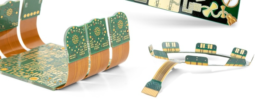
- Choose flexible pcb or flexible printed circuit for compact, bendable applications (e.g., wearable devices)
- Select rigid flex pcb or pcb flex rigid for hybrid rigid-flex needs (e.g., aerospace components)
- Opt for rf pcb or rf circuit board for high-frequency applications (e.g., communication devices), prioritizing low-loss materials
- Use multilayer pcb for complex circuits; upgrade to HDI PCB with high density interconnect and microvia for miniaturized designs
Finalize Design & Gerber Files for Production
Gerber files are the universal language for PCB manufacturing, so accuracy here is non-negotiable
- Convert design files to Gerber format: Include all layers (top/bottom copper, solder mask, silkscreen) for seamless transfer to production
- Add drill files and netlists: Ensure alignment for through-hole and microvia placement, critical for HDI PCB and multilayer pcb
- Validate design files against manufacturing specs: Eliminate errors that cause delays for pcb prototype and professional PCB manufacturing runs
Print: Translate Design to Physical Imaging for PCB
Printing bridges digital design and physical PCB production, with methods varying by DIY PCB and professional PCB manufacturing needs. The step ensures the design is accurately transferred to a printable medium, setting the stage for subsequent imaging and trace formation.
Printing for DIY PCB Projects
DIY PCB relies on accessible printing tools, with toner-based methods delivering consistent results for small-scale prototype circuit board
- Use laser printers for high-contrast prints: Toner adheres better for transfer, avoiding smudging that ruins trace clarity
- Print on glossy paper or transparency film: Ensure 100% opacity to block light during imaging for etch-resistant traces
- Print at 600-1200 DPI resolution: Higher resolution improves trace precision, critical for fine-pitch DIY PCB designs
Printing for Professional PCB Manufacturing (Imaging Prep)
Professional PCB manufacturing uses industrial printing for high-volume, high-precision boards like multilayer pcb, rf pcb and HDI PCB with microvia
- Generate photomasks via industrial printers: Create high-resolution masks for Imaging, aligning with IPC-6012 standards for rigid PCB qualification
- Print alignment marks: Ensure layer alignment for rigid flex pcb, pcb flex rigid and multilayer pcb, preventing short circuits
- Calibrate for material type: Adjust printing parameters for flexible printed circuit substrates vs rigid board materials
Prepare Board: Prep Substrates for PCB Transfer & Etching
Board preparation ensures the copper substrate is ready to receive the design, with cleanliness and surface condition directly impacting transfer and etch quality. Improper preparation causes 25% of DIY PCB failures and reduces yield for professional PCB manufacturing.
Substrate Selection for Target PCB Types
Choose the right substrate to match performance needs for all circuit board variants
- DIY PCB: Use FR-1 or FR-4 copper-clad boards for low-cost prototype circuit board projects
- Professional PCB manufacturing:
- FR-4 for standard rigid PCB and multilayer pcb
- Polyimide for flexible pcb, flexible printed circuit, rigid flex pcb and pcb flex rigid
- PTFE for rf pcb and rf circuit board to minimize signal loss at high frequencies
- Specialized laminates for HDI PCB with high density interconnect and microvia
Step-by-Step Board Preparation Process
Follow standardized steps for consistent results across DIY and professional workflows
- Cut the board to size: Trim copper-clad substrate to match design dimensions, leaving 5mm margin for handling
- Clean the copper surface: Remove oxidation and oil with abrasive pads; wipe with isopropyl alcohol for a grease-free finish
- Polish the surface (optional): Lightly sand for DIY PCB to improve toner adhesion; use chemical cleaning for professional PCB manufacturing
- Dry thoroughly: Avoid moisture that disrupts Transfer and Etching processes for all PCB types
Transfer: Apply Design to Copper Substrate for PCB
Transfer moves the printed design onto the copper substrate, creating a protective layer that resists etching. The method differs drastically between DIY PCB and professional PCB manufacturing, with precision critical for fine traces in rf pcb and HDI PCB.
Transfer Methods for DIY PCB
DIY transfer uses low-cost, accessible techniques ideal for small prototype circuit board projects
- Toner transfer process (most common):
- Align printed design (toner side down) on cleaned copper surface
- Apply heat (180-200°C) and pressure with a heat press or iron for 2-3 minutes
- Peel off paper/transparency slowly while warm to avoid design smudging
- Ensure full coverage: Check for gaps in traces, which cause etching errors and faulty circuits
Transfer for Professional PCB Manufacturing (Imaging)
Professional Imaging uses industrial processes for high-precision, high-volume PCB production
- Photolithography for standard PCB: Expose copper-clad substrate to UV light through photomasks; the unexposed photoresist remains as a protective layer
- Laser direct imaging (LDI) for advanced boards: Use laser to directly image design onto substrate, ideal for HDI PCB, high density interconnect, microvia and multilayer pcb
- Align layers precisely: Critical for rigid flex pcb, pcb flex rigid and multilayer pcb to avoid signal cross-talk and short circuits
Etch: Remove Unwanted Copper for PCB Circuit Traces
Etching removes unprotected copper from the substrate, leaving only the desired circuit traces. The step requires strict control of time and chemical concentration to avoid over-etching, a top issue for both DIY PCB and professional PCB manufacturing.
Etching Process for DIY PCB
DIY etching uses affordable chemicals and manual monitoring for prototype circuit board
- Prepare etchant solution: Use ferric chloride (most common) or ammonium persulfate, mixed per manufacturer ratios
- Submerge the board: Fully immerse the prepped PCB in the solution, agitating gently to speed up etching
- Monitor progress: Check every 2-3 minutes; etching takes 10-20 minutes depending on solution temperature and concentration
- Remove promptly: Stop etching once all unprotected copper is gone to avoid trace damage
Etching & Plating for Professional PCB Manufacturing
Professional processes ensure consistency for high-volume and specialized boards like rf pcb and multilayer pcb
- Automated etching: Use conveyorized systems to control etchant concentration, temperature and time for uniform results
- Plating for conductivity: Add copper plating to reinforce traces and fill vias, critical for HDI PCB with microvia and high density interconnect
- Adhere to IPC-6012: Ensure trace thickness meets standards (minimum 1oz copper for industrial PCB, 2oz for high-current applications)
- Specialized etching for flexible pcb: Use low-stress etchants to avoid substrate damage for flexible printed circuit
Clean & Drill: Refine PCB Substrate for Assembly
Cleaning removes residual etchant and protective layers, while drilling creates holes for components and interconnections. This step is critical for both DIY PCB and professional PCB manufacturing, with precision drilling mandatory for microvia and HDI PCB.
Post-Etch Cleaning for All PCB Types
Thorough cleaning prevents corrosion and ensures proper solder adhesion during Assembly
- Rinse the board: Use running water to wash away residual etchant, critical to avoid trace degradation
- Strip protective layers: Remove toner (DIY) or photoresist (professional) with chemical strippers or isopropyl alcohol
- Dry and inspect: Ensure no residue remains; check for broken traces or under-etching before drilling
Drilling for PCB (Lamination & Drilling for Professional Production)
Drilling methods vary by board complexity, with lamination preceding drilling for multilayer and rigid-flex designs
- DIY PCB drilling: Use a handheld drill with tiny bits (0.5-1.0mm) for through-holes; secure the board to avoid shifting
- Professional Lamination & Drilling:
- Lamination first for multilayer pcb, rigid flex pcb and pcb flex rigid: Bond layers with heat and pressure, adhering to IPC-2221 for layer alignment
- Automated drilling: Use CNC machines for precise through-holes, blind vias and buried vias
- Microvia drilling for HDI PCB: Use laser drilling for 0.05-0.2mm microvia, critical for high density interconnect designs
- Deburr holes: Remove sharp edges to prevent component damage during Assembly
Solder Mask & Silkscreen: Protect and Label PCB
Solder mask and silkscreen add protection and clarity to PCB, extending lifespan and simplifying Assembly. These steps are optional for basic DIY PCB but mandatory for professional PCB manufacturing and specialized boards like rf pcb and rigid flex pcb.
Solder Mask Application for PCB
Solder mask protects copper traces from oxidation and short circuits, with material matching board type
- DIY PCB solder mask: Use spray-on or brush-on solder mask; cure with heat or UV light for 10-15 minutes
- Professional solder mask:
- Apply liquid photoimageable solder mask to the board surface
- Expose and develop to leave mask only on non-trace areas
- Cure at high temperature for permanent protection, critical for flexible pcb and flexible printed circuit durability
- Color selection: Green for standard PCB; red/blue for custom prototype circuit board; matte black for rf pcb to reduce glare
Silkscreen Printing for PCB Identification
Silkscreen adds labels for components, pins and polarity, simplifying Assembly and troubleshooting
- DIY PCB silkscreen: Use stencils and acrylic paint to add basic labels; cure for adhesion
- Professional silkscreen:
- Print component designators, logos and polarity marks via photolithography
- Cure silkscreen ink to resist wear, even for flexible pcb and rigid flex pcb that undergo bending
- Ensure text size is readable (minimum 0.8mm height) for easy Assembly
Testing & Finishing: Validate and Finalize PCB Quality
Testing ensures the PCB meets performance standards, while finishing enhances durability and conductivity. This phase is non-negotiable for professional PCB manufacturing and recommended for all pcb prototype to avoid Assembly failures.
Comprehensive PCB Testing Protocols
Testing varies by board complexity, with rigorous checks for specialized types like rf pcb and HDI PCB
- Basic testing for DIY PCB: Use a multimeter to check for short circuits and open traces; verify continuity across key paths
- Professional Testing & Finishing for all circuit board types:
- Continuity testing: Ensure all traces connect as designed, critical for multilayer pcb and HDI PCB with high density interconnect
- Signal integrity testing: Mandatory for rf pcb and rf circuit board to confirm low loss and minimal interference
- Thermal testing: Check heat dissipation for high-power PCB, adhering to IPC-6012 reliability standards
- Functional testing: Validate performance against design specs for prototype circuit board and production runs
PCB Finishing for Enhanced Performance
Finishing coats protect copper and improve solderability, with options matching application needs
- DIY PCB finishing: Apply tin plating or solder paste to exposed pads for corrosion resistance
- Professional finishing options:
- HASL (Hot Air Solder Leveling): Cost-effective for standard PCB and rigid flex pcb
- ENIG (Electroless Nickel Immersion Gold): Ideal for flexible printed circuit, rf pcb and HDI PCB with microvia for long-term reliability
- OSP (Organic Solderability Preservative): Eco-friendly option for prototype circuit board and low-volume runs
Assemble: Complete PCB to Functional PCA
Assembly transforms bare PCB into a functional PCA, with methods ranging from manual DIY to automated professional processes. Proper assembly prevents component failure, especially for delicate flexible pcb and high-precision HDI PCB.
DIY PCB Assembly for Prototype Circuit Board
Manual assembly is ideal for small-batch DIY PCB projects, with careful handling to avoid damage
- Prepare components: Sort resistors, capacitors, ICs and connectors per design; verify polarity for polarized parts
- Apply solder paste: Use a stencil or toothpick to apply small amounts of solder to pads
- Place components: Align components with footprints; secure with tape for through-hole parts
- Solder components: Use a soldering iron (350-380°C) for precise soldering; avoid overheating to prevent trace damage
- Trim leads: Cut excess component leads for a clean finish; inspect for cold joints or bridges
Professional PCB Assembly for Mass Production
Automated assembly ensures consistency for high-volume professional PCB manufacturing runs
- SMT placement: Use pick-and-place machines for surface-mount components, critical for HDI PCB and microvia-integrated boards
- Reflow soldering: Cure solder paste in a controlled oven for strong, reliable joints
- Through-hole assembly: Use wave soldering for larger components on rigid flex pcb and pcb flex rigid
- Inspection: Deploy AOI (Automated Optical Inspection) to detect defects; rework faulty joints promptly
- Functional testing: Validate assembled PCA performance for end-use applications
DIY PCB vs Professional PCB Manufacturing: Core Differences & Selection Guide
Choosing between DIY PCB and professional PCB manufacturing depends on project scale, precision needs and performance requirements. The following comparison clarifies the best fit for each scenario, resolving common selection dilemmas.
Core Differences: DIY PCB vs Professional PCB Manufacturing (Comparison Table)
| Factor | DIY PCB | Professional PCB Manufacturing |
|---|---|---|
| Scale | Small-batch (1-100 units), ideal for pcb prototype | High-volume (1000+ units) and small-batch precision runs |
| Precision | Moderate (minimum 0.2mm trace width) | High (0.05mm trace width, microvia for HDI PCB) |
| Board Types Supported | Basic rigid PCB, simple prototype circuit board | Rigid, flexible pcb, flexible printed circuit, rigid flex pcb, pcb flex rigid, rf pcb, rf circuit board, multilayer pcb, HDI PCB |
| Compliance | No mandatory standards | IPC-2221, IPC-6012 and industry-specific certifications |
| Turnaround Time | 1-3 days (per batch) | 3-7 days (prototype), 10-14 days (mass production) |
| Cost | Low (per unit: $1-$5) | Low per unit for high volume; moderate for pcb prototype ($5-$20 per unit) |
| Performance | Suitable for low-demand applications | Optimized for high-frequency (rf pcb), high-reliability (rigid flex pcb) and complex (multilayer pcb) use cases |
Selection Framework: When to Choose DIY vs Professional Manufacturing
- Choose DIY PCB when: Project is a prototype circuit board, volume is low, design is simple and cost is a top priority
Choose professional PCB manufacturing when: Requiring flexible pcb, rf pcb, multilayer pcb or HDI PCB with microvia and high density interconnect; needing IPC compliance; targeting high volume or high reliability


![Understanding PCB Costs & Pricing [Your Complete Guide]](https://hdicircuitboard.com/wp-content/uploads/elementor/thumbs/Understanding-PCB-Costs-Pricing-Your-Complete-Guide-qzzhe6mcaxuolkux3xalfktgavumi9y1aqfbs9bpv4.webp "Understanding PCB Costs & Pricing [Your Complete Guide]")


