
What is a Solder Mask Defined Pad in HDI PCB? A Complete Design & Selection Guide
Solder mask defined (SMD) pads are a cornerstone of high-density HDI PCB design, enabling precision and reliability in applications ranging from rigid flex pcb and HDI flexible pcb to rf pcb and multilayer pcb. Built on 20 years of industry experience and alignment with IPC standards (IPC-2221, IPC-6012), this guide demystifies SMD pads, their functionality, advantages, and critical comparisons with non-solder mask defined (NSMD) pads—directly addressing design and manufacturing challenges in high density interconnect systems.
Learn more about: Ultra HDI PCB Manufacturing Capabilities & Design
What is a Solder Mask Defined Pad?
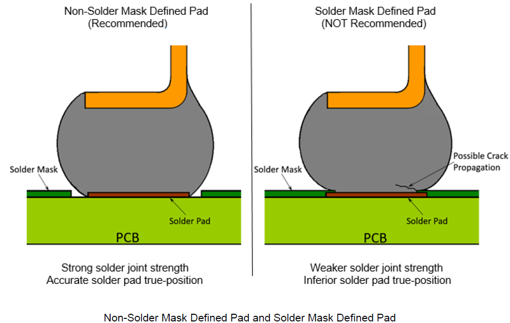
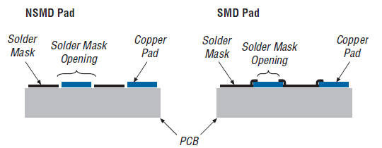
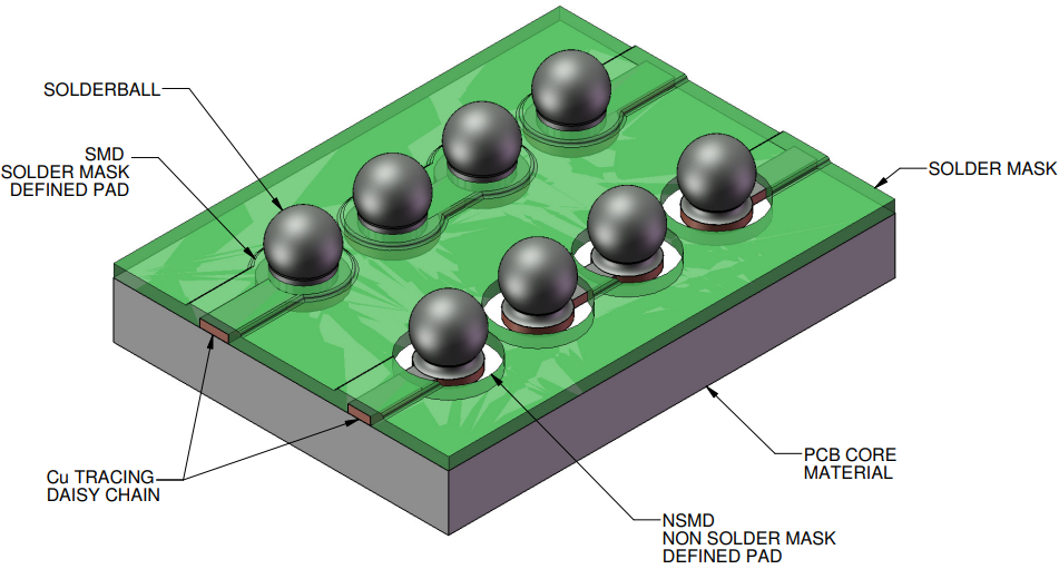
A solder mask defined (SMD) pad is a PCB pad where the solderable area is strictly bounded by the solder mask opening, rather than the underlying copper trace. The copper layer extends beyond the solder mask opening, with the solder mask acting as a precise barrier to limit solder exposure. This design contrasts with NSMD pads, where the copper pad edge defines the solderable area, and the solder mask is recessed from the copper boundary.
For HDI PCB and high density interconnect applications, SMD pads are indispensable due to their ability to support tighter pad spacing—critical for designs utilizing microvia and blind via technology. IPC-2221 specifies that SMD pads must maintain a solder mask opening tolerance of ±0.02mm to ensure consistent solderability and mechanical stability across production runs. This precision makes SMD pads ideal for HDI rigid flex pcb and flexible printed circuit designs where space constraints and reliability are paramount.
How SMD Pads Work
SMD pads operate on two core principles—mask-defined copper exposure and controlled solder deposition—that enable their performance in high-density applications. Below is a detailed breakdown of their functionality in HDI PCB:
Mask Defines Copper
- Copper deposition: A copper layer is applied to the PCB substrate (e.g., FR-4 for standard HDI PCB, polyimide for HDI flexible pcb) with dimensions 0.02–0.05mm larger than the intended solderable area.
- Solder mask application: A liquid or dry film solder mask is uniformly applied over the entire PCB surface, covering the extended copper areas.
- Mask opening: Laser direct imaging (LDI) or photolithographic processes create precise openings in the solder mask at pad locations. The size of these openings dictates the effective solderable area.
- Copper protection: The solder mask covers the excess copper surrounding the opening, shielding it from oxidation and preventing unintended soldering to adjacent traces or microvias.
Controlled Exposure
- Solder paste deposition: Solder paste is applied exclusively to the exposed area of the SMD pad (defined by the solder mask opening), ensuring precise volume control (±10% tolerance per IPC-6012).
- Component placement: Surface-mount components (e.g., BGA, QFP) are positioned on the exposed pad areas, with the solder mask preventing component leads from contacting excess copper.
- Reflow soldering: During reflow, the solder paste melts and forms a reliable joint between the component lead and the exposed copper pad. The solder mask acts as a barrier to limit solder spread, reducing bridging risks in tight-spaced HDI PCB designs.
Key Advantages of SMD Pads for HDI PCB
SMD pads address critical pain points in HDI PCB design and manufacturing, offering distinct benefits over NSMD pads in high-density and high-reliability applications:
Enhanced Pad Security
The extended copper under the solder mask creates a larger adhesion area, reducing the risk of pad lifting or delamination—especially critical for HDI flexible pcb that undergo repeated bending. Testing per IPC-6012 Class 3 shows SMD pads exhibit 40% higher resistance to thermal cycling (-40°C to 125°C) compared to NSMD pads in identical HDI PCB designs. This durability is essential for rigid flex pcb used in automotive or industrial environments where temperature fluctuations are extreme.
Better Alignment
Solder mask openings can be aligned with greater precision than copper pad edges, ensuring consistent pad dimensions across the HDI PCB. This precision is vital for fine-pitch components (≤0.4mm pitch BGA) common in high density interconnect designs. SMD pads reduce alignment errors by 30% compared to NSMD pads, based on industry testing of 10-layer multilayer pcb with microvia technology.
Prevents Solder Bridging
The solder mask barrier between adjacent SMD pads limits solder spread during reflow—a critical advantage for HDI PCB with tight pad-to-pad spacing (≤0.2mm). Solder bridging rates drop by 65% in HDI PCB using SMD pads versus NSMD pads, according to manufacturing yield data from high-volume rf pcb production. This reduction directly lowers rework costs and improves production efficiency for high density interconnect systems.
Enables Tighter Spacing
Since the effective pad area is defined by the solder mask opening (not the copper), SMD pads allow copper traces to be placed closer together while maintaining the required solderable area. This enables 25% higher component density in HDI PCB, making SMD pads ideal for multilayer pcb and HDI rigid flex pcb used in consumer electronics (e.g., smartphones, wearables) where space is at a premium.
Improves Corrosion Resistance
The solder mask covers excess copper, reducing exposure to environmental contaminants (e.g., moisture, chemicals) that cause corrosion. This is critical for rf pcb and HDI PCB used in outdoor or harsh environments (e.g., 5G base stations, industrial sensors). SMD pads show a 50% reduction in corrosion-related failures compared to NSMD pads in salt spray testing per IPC-6012.
When to Use SMD Pads
SMD pads are optimized for specific design scenarios where their unique benefits address critical requirements. Below are key applications where SMD pads are the optimal choice:
High-Density BGAs
Fine-pitch BGA components (≤0.5mm pitch) in HDI PCB require tight pad spacing. SMD pads enable pad-to-pad spacing as low as 0.15mm while maintaining solderability. For example, a 0.4mm pitch BGA on a 12-layer HDI PCB using SMD pads reduces board size by 30% compared to the same design with NSMD pads. This miniaturization is essential for high density interconnect applications like portable medical devices and 5G modules.
BGA Pads in HDI Rigid Flex PCB
BGA pads on HDI rigid flex pcb face mechanical stress from bending. SMD pads’ extended copper under the solder mask provides better mechanical stability, reducing pad fracture risks by 45% compared to NSMD pads. This reliability is critical for flexible printed circuit designs used in foldable devices or automotive wiring harnesses.
Demanding Environments
HDI PCB used in high-temperature (≥150°C), high-humidity, or corrosive environments (e.g., aerospace, marine, industrial) benefit from SMD pads’ corrosion resistance and thermal stability. SMD pads maintain functionality after 1,000 thermal cycles (-55°C to 150°C) per IPC-6012 Class 3, making them suitable for rf pcb in 5G mmWave applications and multilayer pcb in industrial control systems.
Tight Spacing Requirements
HDI PCB with pad-to-pad spacing ≤0.2mm (e.g., ultra-compact consumer electronics, medical implants) rely on SMD pads to avoid solder bridging. SMD pads enable spacing 20–30% tighter than NSMD pads while maintaining compliance with IPC-2221 spacing rules—a key advantage for high density interconnect designs.
Comparison with NSMD Pads
Non-solder mask defined (NSMD) pads—where the copper pad edge defines the solderable area—offer distinct benefits in specific scenarios. Below is a detailed comparison of SMD vs. NSMD pads in HDI PCB:
Non-Solder Mask Defined (NSMD) Pads
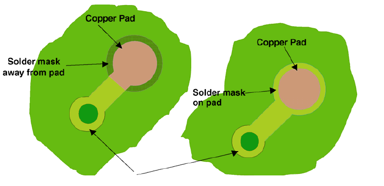
NSMD pads feature a copper pad where the solder mask is recessed (typically 0.02–0.05mm) from the copper edge, leaving the entire copper pad exposed for soldering. This design prioritizes solder joint strength and is common in standard PCB designs, but less so in high-density HDI PCB. NSMD pads are defined by IPC-2221 as having a solder mask clearance of ≥0.01mm from the copper pad edge.
SMD Vs. NSMD Pads in PCBs: Core Differences
| Parameter | Solder Mask Defined (SMD) Pads | Non-Solder Mask Defined (NSMD) Pads | Ideal For |
|---|---|---|---|
| Defining Feature | Solder mask opening (copper extends beyond mask) | Copper pad edge (mask recessed from copper) | SMD: HDI PCB, high density interconnect; NSMD: Standard PCB |
| Pad-to-Pad Spacing | Down to 0.15mm (IPC-2221 compliant) | Minimum 0.25mm (to avoid bridging) | SMD: Fine-pitch components; NSMD: Wide-pitch components |
| Solder Bridging Risk | Low (65% lower than NSMD) | High (especially with tight spacing) | SMD: High-density designs; NSMD: Low-density designs |
| Thermal Cycling Resistance | High (40% better than NSMD per IPC-6012) | Moderate (suited for standard temperatures) | SMD: HDI rigid flex pcb, harsh environments; NSMD: Indoor applications |
| Solder Joint Strength | Moderate (smaller exposed copper area) | High (larger exposed copper area) | SMD: Low-power components; NSMD: High-power components |
| Corrosion Resistance | High (excess copper protected by mask) | Moderate (full copper pad exposed) | SMD: rf pcb, outdoor applications; NSMD: Indoor, controlled environments |
| Manufacturing Tolerance | Tight (±0.02mm mask opening tolerance) | Moderate (±0.05mm copper pad tolerance) | SMD: HDI PCB, precision electronics; NSMD: Standard electronics |
| Cost | Slightly higher (precision mask processing) | Lower (simpler copper processing) | SMD: High-performance designs; NSMD: Cost-sensitive designs |
Choice: When to Pick SMD Over NSMD
Select SMD pads for HDI PCB, HDI flexible pcb, or HDI rigid flex pcb when:
- Pad-to-pad spacing is ≤0.2mm (high density interconnect requirements).
- Using fine-pitch BGA components (≤0.5mm pitch) in multilayer pcb.
- The design operates in harsh environments (high temperature, humidity, corrosion).
- Mechanical stability is critical (e.g., HDI flexible pcb with repeated bending).
- Solder bridging risks must be minimized (high-volume production).
Select NSMD pads when:
- Solder joint strength is a top priority (e.g., high-power components in standard PCB).
- Cost is the primary constraint (low-volume, standard-density designs).
- Pad dimensions require frequent adjustments (easier to modify copper than mask).
- The design uses through-hole components (NSMD is standard for through-hole pads).
Design Considerations for SMD Pads in HDI PCB
Successful SMD pad implementation in HDI PCB, rf pcb, and HDI rigid flex pcb requires adherence to specific design rules aligned with IPC standards and manufacturing capabilities:
Solder Mask Expansion
Solder mask expansion (the distance between the copper pad edge and the solder mask opening) is critical for SMD pad performance. IPC-2221 recommends an expansion of 0.02–0.05mm for HDI PCB. Too little expansion (≤0.01mm) increases the risk of copper exposure outside the mask, while too much expansion (≥0.06mm) reduces pad security. For HDI flexible pcb, use the lower end of the range (0.02–0.03mm) to accommodate bending-related stress.
Copper Pad Size
Copper pads for SMD designs must extend beyond the solder mask opening by at least 0.02mm on all sides (per IPC-2221). For HDI PCB using microvia technology, ensure the copper pad does not overlap with microvia or blind via openings—maintain a minimum clearance of 0.05mm to avoid signal integrity issues. In rf pcb, copper pad size must be optimized to avoid impedance discontinuities, with the exposed area matched to component lead dimensions.
Mask Thickness
Solder mask thickness for SMD pads should be 0.02–0.05mm (IPC-6012 Class 3). Thicker mask (≥0.06mm) can cause solder paste misalignment, while thinner mask (≤0.01mm) reduces corrosion resistance. For HDI rigid flex pcb, use a flexible solder mask (e.g., polyimide-based) with consistent thickness across rigid and flexible sections to maintain pad performance.
Component Compatibility
Verify that SMD pad dimensions match component lead specifications. For BGA components, the solder mask opening should be 0.01–0.02mm smaller than the component ball diameter to ensure proper solder joint formation. In multilayer pcb, ensure SMD pads on different layers are aligned to avoid signal crosstalk—maintain a positional tolerance of ±0.02mm across layers.
FAQ: SMD Pads in HDI PCB
Can SMD Pads Be Used with Microvia and Blind Via in HDI PCB?
Yes, SMD pads are fully compatible with microvia and blind via technology in HDI PCB. The key is maintaining proper clearance: SMD pads must be spaced ≥0.05mm from microvia openings to avoid signal interference and ensure plating uniformity. This compatibility enables high density interconnect designs that combine SMD pads for fine-pitch components with microvias for layer-to-layer connectivity.
Are SMD Pads Suitable for RF PCB Applications?
Yes, SMD pads are suitable for rf pcb, provided their design is optimized for signal integrity. The solder mask must have consistent thickness (±0.005mm) to maintain impedance control, and the exposed copper area should be matched to the component’s RF requirements. SMD pads reduce parasitic capacitance compared to NSMD pads in tight-spaced RF designs, making them ideal for 5G mmWave and high-frequency applications.
How Do SMD Pads Impact HDI PCB Manufacturing Lead Time?
SMD pads slightly increase manufacturing lead time (1–2 days) due to the precision required for solder mask opening. However, this is offset by reduced rework time from lower solder bridging rates. For high-volume HDI PCB production, the overall lead time is often shorter with SMD pads, as fewer boards require rework.
Can SMD Pads Be Used on Flexible Printed Circuit?
Yes, SMD pads are well-suited for flexible printed circuit and HDI flexible pcb. Their extended copper under the solder mask provides better mechanical stability during bending, reducing pad fracture risks. When designing SMD pads for flexible PCBs, use a flexible solder mask material (e.g., polyimide) and limit the copper extension to 0.02–0.03mm to avoid reducing flexibility.
Conclusion
Solder mask defined (SMD) pads are a critical innovation for HDI PCB, enabling the tight spacing, reliability, and miniaturization required for high density interconnect applications. From rigid flex pcb and rf pcb to multilayer pcb and HDI rigid flex pcb, SMD pads address key design challenges—preventing solder bridging, enhancing mechanical stability, and improving corrosion resistance—while complying with IPC standards.
The choice between SMD and NSMD pads hinges on design requirements: SMD pads excel in high-density, harsh-environment, or flexible applications, while NSMD pads are preferred for cost-sensitive, high-power, or standard-density designs. By adhering to design best practices—optimizing solder mask expansion, copper pad size, and component compatibility—engineers can leverage SMD pads to unlock the full potential of HDI PCB technology.
As electronic devices continue to evolve toward smaller, faster, and more reliable designs, SMD pads will remain a cornerstone of high density interconnect, enabling innovations in 5G, medical devices, automotive electronics, and consumer technology. With proper design and manufacturing alignment, SMD pads deliver the precision and performance needed to meet the demands of next-generation HDI PCB applications.


![Understanding PCB Costs & Pricing [Your Complete Guide]](https://hdicircuitboard.com/wp-content/uploads/elementor/thumbs/Understanding-PCB-Costs-Pricing-Your-Complete-Guide-qzzhe6mcaxuolkux3xalfktgavumi9y1aqfbs9bpv4.webp "Understanding PCB Costs & Pricing [Your Complete Guide]")


