
Sequential Lamination in HDI PCB Fabrication: Complete Process, Advantages & Quality Control
Sequential lamination is the foundational manufacturing process for high density interconnect (HDI) PCBs, enabling the creation of compact, high-performance hdi pcb and hdi circuit boards with microvia, blind via, and stacked via structures. This process builds layers incrementally rather than in a single press cycle, supporting the tight geometries and complex interconnections required in modern electronics. Targeted at electronic engineers, PCB procurement teams, and electronics enthusiasts, this guide explains the full sequential lamination workflow, technical requirements, quality control standards, and practical applications—with clear explanations of complex concepts and industry-proven data to support real-world decision-making.
Learn more about: How to Design HDI Microvia PCB
Why Sequential Lamination is Essential for HDI
Sequential lamination overcomes critical limitations of traditional single-step lamination, making it indispensable for HDI PCB technology.
Enablement of Blind and Buried Vias
Traditional lamination only supports through-hole vias, which waste space and introduce signal stubs. Sequential lamination enables:
- Blind Vias: Connect outer layers to inner layers without full-board penetration, eliminating signal reflections in high-speed designs.
- Buried Vias: Link inner layers exclusively, preserving outer routing space for components and fine traces.
- Compliance: Meets IPC-2226 standards for aspect ratio ≤1:1 and alignment tolerance ±0.002″, supporting HDI flexible pcb and HDI rigid flex pcb designs.
Support for Stacked/Staggered Microvias
Microvias (diameter ≤6mil) are the backbone of high-density routing, and sequential lamination enables vertical integration:
- Stacked Microvias: Vertically aligned through multiple build-up layers, increasing routing density by 40–50% compared to standard PCBs. Critical for hdi pcb with fine-pitch BGAs (≤0.4mm).
- Staggered Microvias: Offset to reduce manufacturing complexity, balancing density and cost for mid-range HDI applications.
- Precision: Laser drilling achieves positioning accuracy ±0.001″, meeting IPC-6012 Class 3 for aerospace and medical devices.
Improved Accuracy and Complex Structure Design
Sequential lamination reduces cumulative alignment error and supports advanced architectures:
- Layer Alignment: Incremental build-up maintains ±0.002″ tolerance across 8–14 layer hdi circuit boards, ensuring reliable stacked via connections.
- Complex Stackups: Enables asymmetric and hybrid stackups, including rigid-flex combinations in HDI rigid flex pcb.
- Thickness Control: Build-up layers as thin as 0.1mm allow total board thickness down to 0.8mm for 8-layer HDI PCBs, ideal for portable electronics.
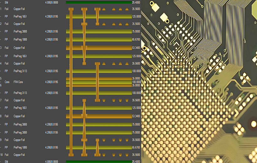
Key Steps in the Sequential Lamination Process
The sequential lamination workflow follows a repeatable, tightly controlled sequence of operations.
Core Preparation & Imaging
The core forms the mechanical backbone of the HDI PCB and requires precise fabrication:
- Material Selection: Core layers use high-Tg FR-4 (Tg ≥180°C) or specialized materials for HDI flexible pcb, with thickness 0.4–0.8mm per IPC-4104.
- Inner Layer Imaging: Dry film photoresist is applied, exposed via photomask, and developed to define traces. Minimum trace width/spacing 3mil/3mil for inner layers per IPC-2221.
- Etching & Inspection: Cupric chloride etchant removes unprotected copper with uniformity ±10%. AOI verifies trace integrity and absence of shorts.
Initial Lamination & Build-Up Cycle
The first lamination cycle establishes the base structure for subsequent layers:
- Pre-preg Preparation: Low-Dk pre-preg (Dk = 3.0–3.8) is cut and placed between the core and outer copper foil (½ oz or 1 oz).
- Lamination Parameters: Temperature 180–200°C, pressure 200–300 psi, time 60–90 minutes to ensure full resin flow and bonding.
- De-burring & Cleaning: The panel is de-burred and plasma-cleaned to improve adhesion for subsequent layers.
Laser Drilling (Microvias)
Laser drilling creates the microvias and blind vias that define HDI interconnect density:
- Laser Selection: UV lasers (355nm) drill microvias 2–6mil in diameter with minimal thermal damage to dielectrics.
- Depth Control: Drill depth is calibrated for blind vias or inter-layer vias, maintaining aspect ratio ≤0.75:1 per IPC-2226.
- Desmearing: Plasma desmearing removes resin residue from hole walls to ensure reliable plating adhesion.
Plating and Filling
Metallization and filling ensure electrical connectivity and mechanical stability:
- Electroless Copper Plating: A thin conductive base layer (0.5–1µm) is deposited on hole walls and surfaces.
- Electrolytic Copper Plating: Additional copper (20–25µm) is applied to meet current-carrying requirements, with thickness variation ≤10% per IPC-6012.
- Via Filling: Stacked microvias and via-in-pads are filled with conductive or non-conductive epoxy to prevent voids and ensure planarity.
Repeated Cycles & Layer Build-Up
Sequential lamination iterates to add layers and increase routing density:
- Cycle Repetition: Each cycle adds 1–2 layers; typical HDI PCBs use 2–4 cycles to reach 8–14 layers.
- Alignment Verification: X-ray systems confirm registration ±0.002″ before each lamination to avoid stacked via misalignment.
- Thermal Management: Inter-cycle cooling reduces residual stress and minimizes warpage in HDI rigid flex pcb and hdi circuit boards.
Final Processing & Quality Control
Final steps ensure the HDI PCB meets performance and reliability standards:
- Surface Finish: ENIG, immersion silver, or OSP is applied to protect copper and enable soldering; ENIG is preferred for HDI flexible pcb.
- Electrical Testing: Flying probe testing verifies continuity, shorts, and impedance using TDR.
- Mechanical Inspection: X-ray checks via filling and alignment; AOI detects trace and solder mask defects.
- Reliability Testing: Thermal cycling (-40°C to 125°C) and humidity testing (85°C/85% RH) validate compliance with IPC-6012 Class 3.
Key Aspects of Sequential Lamination
Process Flow Comparison: Sequential vs. Traditional Lamination
| Aspect | Sequential Lamination | Traditional Single-Step Lamination |
|---|---|---|
| Layer Addition | Incremental (2–4 cycles) | Single cycle (all layers at once) |
| Via Support | Microvia, blind via, stacked via | Through-hole vias only (≥12mil) |
| Alignment Tolerance | ±0.002″ (low cumulative error) | ±0.005″ (higher cumulative error) |
| Component Density | 2–3x higher (supports 0.4mm BGAs) | Lower (limited to ≥0.8mm BGAs) |
| Warpage Risk | Lower (inter-cycle stress relief) | Higher (uniform stress across layers) |
| Typical Use | HDI PCB, HDI flexible pcb, aerospace | Standard multilayer PCBs, industrial controls |
HDI Application Spectrum
Sequential lamination enables high density interconnect across industries:
- Consumer Electronics: 8-layer HDI PCBs with stacked microvias reduce board size by 30–40% in smartphones and wearables.
- Medical Devices: HDI rigid flex pcb with sequential lamination balances flexibility and density for implantable and portable tools.
- Aerospace & Defense: 14-layer hdi circuit boards with blind/buried vias meet strict reliability in extreme environments (-55°C to 125°C).
- Automotive Electronics: ADAS systems use HDI PCBs to support multiple sensors and high-speed data links.
Key Advantages of Sequential Lamination
Density & Miniaturization
- Space Optimization: Stacked microvias and blind/buried vias reduce via footprint by 60–70%, enabling up to 200 components per square inch.
- Size Reduction: HDI PCBs are 30–40% smaller than traditional boards with equivalent functionality, critical for portable devices.
Signal Integrity & Performance
- Shorter Paths: Blind/buried vias eliminate stubs, reducing reflections by 40–50% in high-speed (≥10Gbps) designs.
- Controlled Impedance: Uniform dielectric thickness maintains impedance tolerance ±5% per IPC-2221 for RF and high-speed signals.
Design Flexibility
- Hybrid Stackups: Supports rigid-flex integration and asymmetric layer counts for specialized applications.
- Power Distribution: Dedicated power layers with stacked vias reduce voltage drop by 15–20% compared to traditional PCBs.
Challenges of Sequential Lamination
Manufacturing Complexity & Cost
- Process Complexity: Multiple cycles increase production time by 20–30% vs. traditional lamination.
- Cost Factors: Laser drilling and precision alignment add upfront cost, though volume production (≥1000 units) reduces per-unit cost by 15–20%.
Quality Control Challenges
- Alignment Consistency: Maintaining ±0.002″ tolerance requires advanced X-ray registration and skilled operators.
- Via Filling Defects: Epoxy curing at 180°C for 60 minutes minimizes voids; X-ray rejects boards with voids >5% of via volume.
Material Compatibility
- Dielectric Selection: Low-Dk (3.0–3.8) and low-Df (≤0.005) materials are required, increasing material cost by 25–30% vs. standard FR-4.
- Adhesion: Plasma cleaning and controlled lamination ensure bond strength ≥1.5 lb/in per IPC-TM-650, preventing delamination.
FAQ: Sequential Lamination in HDI PCB Fabrication
What is the difference between PCB and PCA, and how does sequential lamination impact this?
PCB (Printed Circuit Board) refers to the bare substrate with copper traces; PCA (Printed Circuit Assembly) includes mounted components. Sequential lamination enables smaller, denser PCBs, which support more compact PCAs essential for smartphones and wearables.
How to choose between sequential lamination and traditional lamination?
Choose sequential lamination for designs requiring microvia/blind via, 0.4mm+ fine-pitch components, ≥30% size reduction, or high-speed signals (≥10Gbps). Use traditional lamination for cost-sensitive projects with larger components (≥0.8mm pitch) and moderate density.
What is the typical lead time for HDI PCBs using sequential lamination?
Prototypes (1–100 units): 2–3 weeks. Volume production (≥1000 units): 4–6 weeks, due to multiple lamination and testing cycles.
Can sequential lamination be used for HDI flexible pcb and HDI rigid flex pcb?
Yes. Sequential lamination works with polyimide substrates for HDI flexible pcb and enables seamless rigid-flex integration in HDI rigid flex pcb while preserving alignment and signal integrity.
What IPC standards govern sequential lamination?
- IPC-2226: HDI design rules for via dimensions and layer alignment.
- IPC-6012: Performance requirements for rigid PCBs, including copper thickness and reliability.
- IPC-4104: Base material specifications for lamination compatibility.
- IPC-TM-650: Test methods for bond strength, via filling, and thermal reliability.
Conclusion
Sequential lamination is the enabling technology behind modern high density interconnect (HDI) manufacturing, supporting the production of hdi pcb, hdi circuit boards, HDI flexible pcb, and HDI rigid flex pcb with microvia, blind via, and stacked via structures. By building layers incrementally, the process achieves unmatched density, signal integrity, and design flexibility—reducing board size by 30–40% and increasing routing density by 40–50% compared to traditional methods. While sequential lamination introduces greater manufacturing complexity and cost, its performance benefits justify investment in applications from consumer electronics to aerospace and medical devices. Adherence to IPC standards, rigorous quality control, and optimized material selection ensure sequential lamination delivers reliable, production-ready HDI PCBs that meet the demands of today’s high-performance electronics.


![Understanding PCB Costs & Pricing [Your Complete Guide]](https://hdicircuitboard.com/wp-content/uploads/elementor/thumbs/Understanding-PCB-Costs-Pricing-Your-Complete-Guide-qzzhe6mcaxuolkux3xalfktgavumi9y1aqfbs9bpv4.webp "Understanding PCB Costs & Pricing [Your Complete Guide]")


