
General Cleaning: Routine Maintenance for PCB Longevity
General cleaning targets surface debris, dust, and light flux residues that accumulate during manufacturing, assembly, or regular use. This process preserves signal integrity, prevents overheating, and extends the lifespan of all PCB types—from basic single-layer boards to complex hdi circuit boards and flexible printed circuit designs.
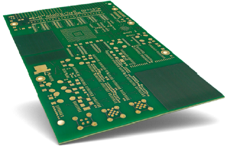
Learn more about :What Is a PCB?
Key Objectives of General Cleaning
- Remove dust, lint, and loose particles that block heat dissipation
- Eliminate light flux residues left after soldering or rework
- Maintain electrical conductivity between traces, components, and microvias
- Prevent buildup that can lead to short circuits or corrosion over time
- Comply with IPC-A-610 standards for electronic assembly cleanliness
Suitable Applications
- Post-assembly cleaning for multilayer pcb and rf pcb
- Routine maintenance for industrial control boards and consumer electronics
- Pre-inspection cleaning before PCB testing or rework
- Cleaning of rigid flex pcb and flexible pcb after bending or installation
Disconnect Power & Remove Parts: Pre-Cleaning Preparation
Step-by-Step Preparation
- Unplug the circuit board from all power sources and external connections
- Remove batteries or power modules to eliminate residual voltage
- Detach removable components (e.g., connectors, sensors, daughterboards) using proper tools
- Document component positions with photos or labels to ensure correct reinstallation
- Place the PCB on an anti-static mat to prevent electrostatic discharge (ESD) damage
- Cover sensitive areas (e.g., connectors, microvias, blind vias) with masking tape if targeted cleaning is needed
Considerations for Specialized PCBs
- Flexible pcb: Support the board with a flat surface to avoid bending or creasing during cleaning
- Hdi pcb: Handle with non-latex gloves to prevent oil transfer to dense component arrays
- Rigid flex pcb: Avoid applying pressure to flex-rigid transition points during part removal
- Rf pcb: Use ESD-safe tools to protect sensitive radio frequency components
Apply Isopropyl Alcohol: Primary Cleaning Agent
Application Techniques
- Pour 90-99% isopropyl alcohol (IPA) into a clean, lint-free spray bottle or container
- For targeted cleaning, apply IPA to a microfiber cloth or cotton swab instead of direct spraying
- Saturate the cloth or swab lightly—avoid dripping alcohol into blind vias or component gaps
- For large PCBs or multilayer pcb, use a soft-bristled brush to distribute IPA over traces and components
- Allow IPA to sit for 30-60 seconds to dissolve flux residues and grime
Benefits of IPA for PCB Cleaning
- Fast-evaporating formula leaves no residue on hdi pcb or flexible printed circuit surfaces
- Non-conductive when pure, reducing short-circuit risks during cleaning
- Effective at dissolving rosin-based and no-clean flux residues
- Compatible with all standard PCB materials (FR4, polyimide, copper traces)
- Safe for use on sensitive components and microvias when applied correctly
Wipe & Dry: Removing Residues and Moisture
Wiping Process
- Use a lint-free microfiber cloth to wipe the PCB surface in one direction (avoid circular motions)
- Use cotton swabs to clean tight spaces around components, blind vias, and microvias
- For flexible pcb, wipe gently along the direction of the flex to prevent trace damage
- Replace cloths or swabs frequently to avoid re-depositing residues
- Focus on high-residue areas (e.g., solder joints, component leads, via openings)
Drying Techniques
- Allow the PCB to air-dry in a well-ventilated area for 10-15 minutes
- Use compressed air (regulated to 30-40 PSI) to blow moisture from blind vias and component gaps
- For hdi pcb and high-density designs, direct compressed air at a 45-degree angle to microvias
- Avoid heat sources (e.g., hair dryers) as excessive heat can damage solder joints or flexible materials
Corrosion Removal: Addressing Rust and Oxidation
Identifying Corrosion Types
- Green/blue corrosion: Typically from copper oxidation or battery leakage (common in consumer electronics)
- White/powdery corrosion: Result of moisture exposure or flux residue buildup
- Black corrosion: Indicates severe oxidation, often affecting trace conductivity
- Targeted removal required for hdi pcb and microvias to avoid trace damage
Tools for Corrosion Removal
- Soft-bristled brushes (nylon or brass) for gentle scrubbing
- Dental picks or plastic scrapers for precision cleaning around components
- Microfiber swabs for accessing blind vias and tight spaces
- Magnifying glass or microscope for inspecting corrosion on high density interconnect (HDI) designs
Neutralize with Baking Soda: Safe Corrosion Treatment
Preparation and Application
- Mix 2 parts baking soda with 1 part water to create a thick paste
- Apply the paste directly to corroded areas using a cotton swab or small brush
- Allow the paste to sit for 5-10 minutes to neutralize acidic corrosion (e.g., from battery leakage)
- For stubborn corrosion on multilayer pcb, reapply the paste and gently agitate
- Avoid applying paste to microvias or blind vias—use a pinpoint swab for precision
Advantages of Baking Soda
- Non-abrasive formula won’t scratch copper traces or solder masks
- Neutralizes acidic residues without damaging components or flexible pcb substrates
- Cost-effective alternative to commercial corrosion removers
- Safe for use on all PCB types, including rf pcb and rigid flex pcb
- Easy to rinse away, leaving no residual film
Scrub & Rinse: Removing Neutralized Corrosion
Scrubbing Techniques
- Use a soft-bristled brush to gently scrub the baking soda paste over corroded areas
- Apply light pressure to avoid damaging traces, especially on flexible pcb and hdi pcb
- For large corroded regions, use a microfiber cloth to wipe in straight, gentle strokes
- Focus on solder joints and component leads where corrosion commonly accumulates
- Inspect microvias and blind vias with a magnifying glass to ensure full cleaning
Rinsing Process
- Rinse the PCB under lukewarm (not hot) deionized water to remove paste and corrosion
- For high density interconnect (HDI) pcb, use a gentle stream of water directed at via openings
- Avoid soaking the PCB—rinse quickly to prevent water penetration into component housings
- For flexible printed circuit designs, pat dry immediately after rinsing to prevent warping
- Repeat rinsing if residue remains, especially around blind vias or dense component arrays
Dry Thoroughly: Preventing Post-Cleaning Damage
Comprehensive Drying Methods
- Use compressed air to blow water from all surfaces, focusing on blind vias, microvias, and component gaps
- Place the PCB on a clean, dry towel in a well-ventilated area for 20-30 minutes
- For critical applications (e.g., rf pcb, medical device PCBs), use a low-temperature oven (60-80°C) for 30 minutes
- Use desiccant packs in a sealed container to absorb remaining moisture for 2-4 hours
- Verify dryness with a multimeter—check for conductivity between unrelated traces to ensure no water remains
Drying Considerations for Specialized PCBs
- Flexible pcb: Lay flat during drying to maintain shape; avoid hanging or bending
- Hdi pcb: Ensure microvias are fully dry to prevent moisture-induced corrosion
- Rigid flex pcb: Dry flex and rigid sections separately to avoid warping transition points
- Multilayer pcb: Allow extra drying time for inner layers, which retain moisture longer
Use the Right Alcohol: Selecting the Correct IPA Concentration
Alcohol Concentration Guide
| Concentration | Best For | Limitations |
|---|---|---|
| 99% IPA | Heavy flux residue, corrosion cleaning, hdi pcb | Fast evaporation requires quick wiping; higher cost |
| 90% IPA | General cleaning, post-soldering residue | Balances evaporation speed and effectiveness |
| 70% IPA | Light dust and grime, routine maintenance | Slower evaporation; may leave slight moisture if not dried properly |
| <70% IPA | Not recommended for PCB cleaning | High water content increases drying time and corrosion risk |
Alcohol Selection Factors
- Choose 99% IPA for hdi pcb and high-density designs to minimize moisture exposure
- Use 90% IPA for most general cleaning tasks to balance performance and cost
- Avoid denatured alcohol or rubbing alcohol with additives (e.g., fragrance, moisturizers)
- Ensure alcohol is labeled “electronics-grade” to avoid contaminants that damage traces
- Store alcohol in a sealed container to prevent water absorption, which reduces effectiveness
Avoid Harsh Cleaners: Protecting PCB Integrity
Prohibited Cleaning Agents
- Acetone: Dissolves solder mask and damages flexible pcb substrates
- Bleach: Corrodes copper traces and components; leaves toxic residues
- Ammonia-based cleaners: Damages plastic components and degrades solder joints
- Abrasive cleaners (e.g., scouring pads, toothpaste): Scratches traces and solder mask
- Petroleum-based solvents: Leave sticky residues and damage polyimide in flexible printed circuit designs
Risks of Harsh Cleaners
- Shortened PCB lifespan due to material degradation
- Reduced signal integrity on rf pcb and high-speed circuits
- Microvia and blind via clogging from residue buildup
- Component failure from chemical damage to leads or housings
- Non-compliance with IPC-6012 standards for PCB quality
Protect Sensitive Parts: Targeted Cleaning Strategies
Sensitive Component Protection
- Cover connectors, sensors, and ICs with masking tape before cleaning
- Use cotton swabs instead of spraying to avoid getting alcohol into component housings
- For hdi pcb, use a pinpoint swab to clean around microvias without spreading moisture
- Remove delicate components (e.g., oscillators, LEDs) before heavy cleaning or corrosion treatment
- Use ESD-safe tools when handling sensitive components to prevent static damage
Protection for Specialized PCB Features
- Microvias and blind vias: Use compressed air to clear debris instead of scrubbing
- Flexible pcb traces: Avoid pressure during wiping to prevent cracking
- Rf pcb antennas: Use gentle wiping motions to preserve impedance characteristics
- High density interconnect (HDI) pads: Clean with a dry brush first to remove loose debris before applying alcohol
Professional Cleaning: Industrial-Grade Methods
Professional Cleaning Techniques
- Ultrasonic cleaning: Uses high-frequency sound waves to remove residues from blind vias and microvias; ideal for multilayer pcb and hdi circuit boards
- Inline flux removers: Automated systems for high-volume production; cleans PCBs during assembly
- Batch flux removers: Immersive cleaning for small to medium production runs
- Plasma cleaning: Removes organic contaminants without chemicals; used for critical applications (e.g., medical, aerospace PCBs)
- Vapor degreasing: Uses solvent vapors to clean complex hdi pcb designs without physical contact
Benefits of Professional Cleaning
- Compliance with strict industry standards (IPC-A-610, ISO 13485 for medical devices)
- Consistent results for high-volume PCB production
- Deep cleaning of microvias and blind vias inaccessible with manual methods
- Safe for delicate components and specialized PCBs (rf pcb, rigid flex pcb)
- Reduced risk of damage compared to DIY methods for complex designs
FAQ: Common PCB Cleaning Questions
Can I clean a PCB without isopropyl alcohol?
- Yes—alternatives include electronic-grade citrus-based cleaners, deionized water (for light cleaning), or baking soda paste (for corrosion). Avoid household cleaners.
How often should I clean a circuit board?
- Routine maintenance: Annually for consumer electronics; quarterly for industrial PCBs
- Post-assembly: After soldering or rework to remove flux residues
- After exposure to moisture, dust, or chemicals: Immediately to prevent corrosion
Is it safe to clean a wet PCB?
- Yes—disconnect power first, then clean with IPA and dry thoroughly. Avoid applying power until the board is completely dry.
Can I use a toothbrush to clean a PCB?
- Use only soft-bristled toothbrushes (new, unused) for gentle scrubbing. Avoid hard-bristled brushes that scratch traces or solder mask.
How to clean a flexible printed circuit without damaging it?
- Use 90% IPA on a microfiber cloth, wipe gently along the flex direction, avoid bending during cleaning, and air-dry flat.
Final Inspection & Reassembly
After cleaning and drying, inspect the PCB to ensure optimal results:
- Use a magnifying glass to check for remaining residues, corrosion, or damage to traces
- Verify continuity between critical traces with a multimeter
- Reinstall components in their documented positions, following proper ESD protocols
- For hdi pcb and rf pcb, perform signal integrity testing to confirm performance
- Document the cleaning process for compliance with quality standards (e.g., IPC-A-610)
Proper cleaning preserves the functionality and longevity of all PCB types—from basic circuit boards to advanced hdi pcb and flexible printed circuit designs. By following these methods, you ensure optimal performance, prevent premature failure, and maintain compliance with industry standards for electronic assembly.


![Understanding PCB Costs & Pricing [Your Complete Guide]](https://hdicircuitboard.com/wp-content/uploads/elementor/thumbs/Understanding-PCB-Costs-Pricing-Your-Complete-Guide-qzzhe6mcaxuolkux3xalfktgavumi9y1aqfbs9bpv4.webp "Understanding PCB Costs & Pricing [Your Complete Guide]")


