
How Does High Density Interconnect (HDI) Impact BGA Fanout and Component Placement?
Electronic engineers and PCB sourcing teams regularly face critical bottlenecks with fine-pitch BGAs on traditional circuit boards. Routing escape channels for 0.4mm pitch or smaller BGAs often requires excessive layers, causes signal integrity loss, and drives low production yield. Procurement teams struggle with cost imbalances: higher layer counts increase material expenses, while poor fanout design leads to high scrap rates during assembly. These pain points are especially pronounced in high-speed electronics, consumer devices, and industrial hardware produced in California and across North America. High density interconnect (HDI) resolves these limitations through microvia structures, fine-line routing, and optimized layer stackups that redefine BGA fanout and component placement capability.
Learn more about: How to Design HDI Microvia PCB
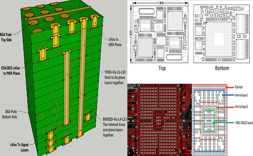
HDI Impact on BGA Fanout Design
Fanout Routing Efficiency – Measurable Space and Layer Reduction
HDI restructures BGA fanout by replacing through-hole vias with microvias and enabling ultra-fine routing, directly improving escape routing density.
- Traditional PCBs rely on 3–4 mil trace/space and through-hole vias, limiting fanout to one or two escape rows for 0.4mm pitch BGAs.
- HDI with 1+N+1 stackup uses 2 mil trace/space and 75μm microvias, supporting three full escape rows and reducing routing area by 35%.
- Any-layer HDI supports via-in-pad (VIP) technology, eliminating dog-bone fanout entirely and reducing fanout radius by 50%.
- IPC-6016 specifies a maximum microvia aspect ratio of 0.8:1 for reliable mass production, allowing 75μm diameter vias with a maximum depth of 60μm.
Signal Integrity & Reliability – Controlled Impedance and Reduced Parasitics
HDI fanout design delivers consistent improvements in high-speed performance and long-term durability.
- Shorter trace lengths in HDI fanout reduce impedance variation by ±5Ω, supporting stable performance for DDR5, PCIe 4.0, and PCIe 5.0 systems.
- Microvias reduce parasitic inductance from approximately 1.0nH to below 0.1nH, lowering signal reflection by over 40%.
- IPC-2226 Class 3 requires trace spacing equal to trace width in HDI designs, limiting crosstalk to below -40dB.
- Thermal cycling tests (IPC-TM-650 2.6.7) show HDI microvia fanout structures maintain stable resistance after 2000 cycles, while through-hole fanout shows 15–20% higher degradation.
Design Tradeoffs – Density, Cost, and Yield Comparison
| Parameter | Conventional PCB Fanout | HDI 1+N+1 Fanout | Any-Layer HDI Fanout |
|---|---|---|---|
| Minimum Supported BGA Pitch | 0.5 mm | 0.4 mm | 0.25 mm |
| Minimum Trace/Space | 3 / 3 mil | 2 / 2 mil | 1 / 1 mil |
| Microvia Diameter | N/A | 75 μm | 50 μm |
| Production Yield | 92–95% | 85–90% | 70–75% |
| Cost Increase vs Standard | 0% | +10–15% | +40–50% |
| Layer Reduction Benefit | N/A | 25–30% | 40–50% |
Tradeoffs in production include lower yield for ultra-fine HDI structures, offset by smaller board size, fewer layers, and lower assembly cost in high-volume runs.
Learn more about: Ultra HDI PCB Manufacturing Capabilities & Design
HDI Impact on Component Placement
Density & Miniaturization – Higher Component Count in Smaller Area
HDI enables dramatic improvements in component density without sacrificing electrical performance or reliability.
- HDI boards support double-sided placement for 0.2mm pitch BGAs, increasing usable board density by 45%.
- 0201 and 01005 passive components can be placed within BGA fanout zones, reducing overall board footprint by 25–30%.
- High-density HDI allows multiple BGAs to be placed in tight clusters, a configuration not feasible on traditional PCBs.
Manufacturing Constraints – Precision Requirements from PCB Fabrication View
From a factory engineering perspective, HDI imposes tighter process controls for component placement.
- Placement accuracy must reach ±0.05 mm for 0.4mm pitch BGAs, compared to ±0.1 mm for traditional PCBs.
- Laser Direct Imaging (LDI) is required for trace/space below 2 mil, increasing setup precision but adding process cost.
- Thermal vias of 60–80μm diameter must be integrated near high-power components to maintain heat dissipation within 5W/cm².
- Lead-free reflow requires temperature control within ±2°C to avoid microvia plating damage, stricter than the ±3°C tolerance for standard PCBs.
Supply Chain Alignment – California HDI PCB Manufacturing Standards
California-based manufacturing follows strict compliance and performance standards for HDI BGA design.
- Production adheres to IPC-6012 and IPC-6016 for microvia reliability and copper plating thickness (minimum 12μm).
- Regional environmental standards require lead-free assembly and halogen-free materials in many high-reliability applications.
- Silicon Valley-driven demand emphasizes 0.25mm pitch BGA support, any-layer HDI, and impedance control for high-speed computing.
- Quality systems include 100% AOI, X-ray inspection for BGA joints, and electrical test for fanout open/short circuits.
Real Factory Production Case Study
Board Specifications
- Type: 10-layer 2+N+2 HDI printed circuit board
- Application: Industrial high-speed controller
- BGAs: Three pieces of 0.3mm pitch BGA
- Trace/Space: 2 / 2 mil
- Microvia size: 75μm diameter, aspect ratio 0.75:1
- Material: Standard FR-4 with 60μm prepreg
Initial Issues
- Fanout routing caused 12% yield loss due to microvia voiding
- Component placement near fanout zones created solder bridging
- Signal crosstalk exceeded acceptable limits during high-speed testing
Corrections and Results
- Adjusted microvia depth to maintain aspect ratio below 0.8:1
- Increased clearance between pads and vias to 0.1mm per IPC-A-610 Class 3
- Optimized ground plane placement to reduce crosstalk
- Final yield improved from 83% to 91%
- Board area reduced by 26% compared to previous conventional design
Common Design Errors from PCB Manufacturing Perspective
- Microvia Aspect Ratio Exceeded: Designs using 75μm vias with 80μm dielectric create ratios above 1:1, leading to 30% more plating voids.
- Insufficient Via-in-Pad Filling: Unfilled VIP traps solder paste during reflow, causing BGA head-in-pillow defects and 8–10% assembly loss.
- Excessive Trace Necking: Narrowing traces below 1 mil for fanout increases etching defects by 25% in mass production.
- Missing Ground Reference Planes: BGA fanout routes without adjacent ground planes increase crosstalk by up to 40% in high-speed signals.
Frequently Asked Questions
- What is the smallest BGA pitch that HDI can support in mass production?
Any-layer HDI reliably supports 0.25mm pitch BGAs with 50μm microvias and 1 mil trace/space. 1+N+1 HDI is the most cost-effective solution for 0.4mm pitch BGAs.
- How does HDI fanout affect BGA rework and repair?
Via-in-pad HDI reduces rework success rate by approximately 15% compared to traditional fanout. X-ray-guided rework stations can restore success rates to acceptable levels for high-reliability products.
- Can HDI reduce overall BGA assembly cost despite higher material expenses?
Yes. For volumes above 10,000 units, 2+N+2 HDI reduces total cost by 12% on average due to fewer layers, smaller board size, and faster assembly cycle time.
- What is the practical difference between stacked and staggered microvias in BGA fanout?
Stacked microvias save 20% routing space but require full copper filling and add cost. Staggered microvias deliver 5–7% higher production yield and do not require filling for 0.4mm pitch BGA designs.
Conclusion
High density interconnect (HDI) fundamentally reshapes BGA fanout and component placement by enabling finer traces, smaller microvias, optimized layer stackups, and significantly higher routing density. Traditional circuit boards cannot reliably support fine-pitch BGAs below 0.5mm, but HDI technologies—including 1+N+1, 2+N+2, and any-layer structures—provide scalable solutions from cost-effective consumer designs to high-performance industrial and computing hardware. By following IPC-2226, IPC-6012, and IPC-6016 standards, controlling microvia aspect ratios, and aligning fanout strategy with real manufacturing capabilities, engineers and procurement teams achieve stable, high-yield production of advanced HDI printed circuit boards. The result is smaller form factors, better signal integrity, fewer layers, and improved cost efficiency in modern electronic hardware systems.


![Understanding PCB Costs & Pricing [Your Complete Guide]](https://hdicircuitboard.com/wp-content/uploads/elementor/thumbs/Understanding-PCB-Costs-Pricing-Your-Complete-Guide-qzzhe6mcaxuolkux3xalfktgavumi9y1aqfbs9bpv4.webp "Understanding PCB Costs & Pricing [Your Complete Guide]")


