
How to Balance Miniaturization, Cost, and Reliability in High Density Interconnect (HDI) Design?
Electronic engineers and PCB sourcing specialists face consistent conflicts in HDI implementation. Shrinking product form factors demand finer features, while production teams struggle with low yields and rising manufacturing costs. Many designs either over‑prioritize miniaturization and suffer reliability failures, or overengineer for durability and exceed budget limits. These conflicts create delays, scrap losses, and missed market windows—especially in volume production environments. High density interconnect (HDI) technology offers solutions, but only when balanced using manufacturable parameters, industry standards, and real factory constraints.
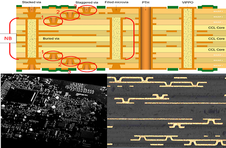
Learn more about: Cost Differences Between 1+N+1, 2+N+2, and Any-Layer High Density Interconnect (HDI) PCBs
Miniaturization – Achievable Density with Manufacturing Stability
Trace and Microvia Scaling
Miniaturization relies on controlled scaling of conductive lines and vertical interconnects, with strict limits based on mass-production capability.
- 2 mil (50 μm) trace and space for 1+N+1 HDI structures, supported by standard laser imaging and 0.5 oz copper plating, delivers consistent yields of 85–90% under IPC‑2226 Class 2 guidelines.
- 1 mil (25 μm) trace and space for any‑layer HDI enables extreme density but requires modified semi‑additive processing and ultra‑thin copper foils, reducing production yield to 70–75%.
- 75 μm microvias with aspect ratio ≤0.8:1 represent the most reliable standard for 1+N+1 HDI, supporting 0.4 mm pitch BGA fanout without excessive defect rates.
- 50 μm microvias enable 0.25 mm pitch BGA routing but require UV laser drilling and tighter dielectric control to avoid plating voids.
Form Factor Optimization
Strategic layout and stacking methods reduce board area without sacrificing stability.
- Dual‑sided component placement increases usable board density by up to 45% compared to single‑sided layouts, supporting 0201 and 01005 passive components.
- Via‑in‑pad (VIP) technology eliminates traditional fanout routing, reducing BGA escape zone size by 50% for compact wearable and mobile designs.
- Sequential build‑up lamination reduces overall board thickness by approximately 20% compared to conventional multilayer structures.
Cost Control – Tradeoffs in HDI Production
Material and Process Cost Levers
Material selection and manufacturing methods directly drive cost without proportional improvements in performance.
- Standard FR‑4 substrates with Tg 130°C support 2 mil trace and space at roughly half the cost of high‑frequency low‑loss materials.
- Low‑loss dielectrics improve signal performance at frequencies above 10 GHz but increase material expenses significantly.
- Staggered microvia structures reduce processing cost by approximately 20% and improve yield by 6–8% compared to stacked microvias.
- Laser Direct Imaging (LDI) improves registration accuracy for fine lines but increases setup cost compared to conventional contact imaging.
Yield‑Driven Cost Reduction
Cost efficiency comes from minimizing scrap rather than reducing specification values.
- Maintaining trace widths above 1.5 mil for non‑critical signal paths reduces etching defects by more than 20%.
- Using 75 μm microvias as a default reduces voiding risks compared to 50 μm vias without major losses in density.
- Automated optical inspection and X‑ray inspection add minimal per‑unit cost but reduce field failure rates and warranty expenses.
- Statistical process control for etching maintains consistent trace dimensions and improves overall production yield.
Reliability – Mitigating Risks in HDI Design
IPC and Regulatory Compliance
Reliability begins with compliance to widely accepted industry and regional standards.
- IPC‑6012 Class 2 requires minimum 12 μm copper plating for microvias and controls for solder joint voiding in commercial electronics.
- IPC‑6012 Class 3 imposes stricter requirements for medical, aerospace, and automotive applications, including enhanced plating thickness and thermal cycle performance.
- Regional environmental regulations mandate lead‑free surface finishes and controlled material compositions for high‑volume markets.
- Thermal cycle testing per IPC‑TM‑650 2.6.7 validates long‑term stability under temperature fluctuations.
Design for Reliability (DFR) Practices
Engineered reliability reduces failure rates without excessive cost.
- Thermal vias ranging from 60 μm to 80 μm in diameter dissipate heat from high‑power components and BGA locations.
- Controlled impedance routing maintains signal quality and reduces electromagnetic interference in high‑speed circuits.
- Adjacent ground planes minimize crosstalk and improve signal integrity for differential and high‑frequency traces.
- Copper plane distribution improves thermal management and structural stability during assembly and operation.
Balancing Strategies – Industry‑Specific Applications
Aerospace and Medical HDI
Reliability takes priority over extreme miniaturization in high‑criticality applications.
- 2 mil trace and space, 75 μm microvias, and 2+N+2 stackups provide stable performance under IPC‑A‑610 Class 3 requirements.
- High‑temperature substrates resist thermal stress in extreme operating environments.
- Full X‑ray inspection and thermal cycle validation ensure zero critical defects in finished assemblies.
Consumer Electronics HDI
Balanced density and cost define successful consumer HDI implementations.
- 1+N+1 stackups with 2 mil trace and space offer predictable yield and manageable cost premiums.
- FR‑4 materials and standard surface finishes balance performance and affordability.
- Controlled use of via‑in‑pad technology reduces size without excessive production risk.
Data Center HDI
High‑speed performance and reliability drive design decisions in computing hardware.
- 1.5 mil trace and space with controlled impedance supports multi‑Gbps data transmission.
- Low‑loss materials preserve signal quality at high frequencies.
- Any‑layer structures enable dense BGA placement while maintaining thermal and electrical stability.
Real Factory Production Case Study
Board Specifications
- Type: 8‑layer 2+N+2 HDI printed circuit board
- Application: Automotive sensor module
- Key parameters: 2 mil trace/space, 75 μm stacked microvias, FR‑4 Tg 150°C, ENIG surface finish
Initial Issues
- Microvia voiding exceeded acceptable limits, causing 18% yield loss
- Signal crosstalk levels fell outside acceptable ranges
- Thermal hotspots appeared under BGA locations during functional testing
Corrections and Results
- UV laser drilling replaced standard laser processes, reducing voiding to acceptable levels
- Ground plane placement improved crosstalk performance
- Additional thermal vias reduced component operating temperatures
- Etch parameter optimization stabilized trace dimensions
Final Outcomes
- Production yield improved from 82% to 92%
- Per‑unit cost decreased by 12%
- The design met all reliability and environmental requirements
Common Design Errors from a Manufacturing Perspective
- Exceeding microvia aspect ratio beyond 0.8:1 creates significant plating voiding and reliability risks.
- Insufficient via‑in‑pad filling leads to solder defects and BGA assembly failures.
- Extreme trace neck‑down below 1.2 mil increases etching defects and reduces production yield.
- Missing ground reference planes between signal layers elevates crosstalk and electromagnetic interference.
- Over‑specifying high‑performance materials for low‑speed circuits creates unnecessary cost without performance gains.
Frequently Asked Questions
- What trace and space combination offers the best balance of miniaturization, cost, and yield?
2 mil (50 μm) trace and space with a 1+N+1 HDI stackup provides the most consistent balance for high‑volume production.
- How does microvia size influence reliability and cost?
75 μm microvias offer the best combination of density, yield, and cost for most applications. Smaller vias increase density but reduce yield and raise cost.
- Can standard FR‑4 materials support reliable HDI miniaturization?
Yes, FR‑4 reliably supports 2 mil trace/space and 75 μm microvias in 1+N+1 HDI structures for most commercial applications.
- How can manufacturers improve HDI reliability without major cost increases?
Controlling aspect ratios, optimizing layer stackups, and implementing consistent inspection processes deliver reliability gains without proportional cost growth.
Conclusion
Balancing miniaturization, cost, and reliability in high density interconnect (HDI) design requires data‑driven decisions rooted in manufacturing capability, industry standards, and application requirements. Over‑reliance on extreme miniaturization leads to low yields and high failure rates, while excessive caution limits innovation and increases board size. By using manufacturable trace and microvia dimensions, selecting appropriate materials, and applying design for reliability principles, engineers and procurement teams create HDI printed circuit boards that meet size, cost, and performance targets simultaneously. Successful HDI implementation depends not on pushing every parameter to its limit, but on creating a stable, repeatable balance that supports volume production and long‑term performance.


![Understanding PCB Costs & Pricing [Your Complete Guide]](https://hdicircuitboard.com/wp-content/uploads/elementor/thumbs/Understanding-PCB-Costs-Pricing-Your-Complete-Guide-qzzhe6mcaxuolkux3xalfktgavumi9y1aqfbs9bpv4.webp "Understanding PCB Costs & Pricing [Your Complete Guide]")


