
How to Calculate Impedance for High Density Interconnect (HDI) PCBs
Challenges in HDI Impedance Control
Even minor impedance deviations on high density interconnect PCBs create direct production and reliability risks:
- A 3Ω to 5Ω shift at 10Gbps–25Gbps increases signal reflection above 10%
- Microvias and ultra‑thin dielectrics in HDI boards amplify sensitivity to geometry changes
- Inconsistent impedance causes 15%–25% yield loss in high‑speed HDI printed circuit boards
- Many designs fail IPC‑6012 Class 2/3 qualification due to uncompensated stack‑up effects
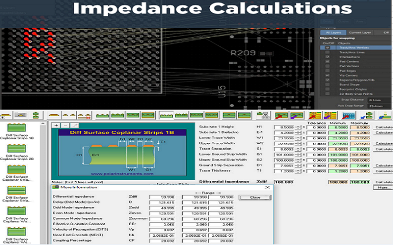
This document provides factory‑validated methods to calculate, control, and stabilize impedance on any HDI PCB.
Learn more about: Learn more about: Signal Integrity in HDI PCB Design
Core Technical Parameters & Calculation Foundations
What Is Controlled Impedance for HDI Boards?
Definition & Industry Standards
Controlled impedance is the consistent characteristic impedance of transmission lines on HDI PCBs, maintained within tight tolerances across signal traces, vias, and layer transitions.
- Defined by IPC‑2221 and IPC‑6012
- Standard tolerance: ±10% for consumer HDI
- High‑speed tolerance: ±5% for 10Gbps+ signals
- Measured in ohms (Ω)
Why HDI Requires Stricter Impedance Control
- Finer traces: 3–8mil instead of 8–12mil on standard PCBs
- Thinner dielectrics: 2–8mil instead of 6–14mil
- Microvias introduce parasitic inductance and capacitance
- Dense routing increases coupling and crosstalk effects
Learn more about:How to Design HDI Microvia PCB
Input Parameters for HDI Impedance Calculation
Mandatory Geometric & Material Parameters
- Trace width (W): 3–8mil for HDI signals
- Trace thickness (T): 0.5oz (17μm) to 1oz (35μm)
- Dielectric height (H): 2–8mil between signal and reference plane
- Dielectric constant (Dk): 3.2–4.2 at operating frequency
- Trace spacing (S): 4–10mil for differential pairs
- Microvia diameter: 6–12mil (laser‑drilled)
- Solder mask thickness: 0.5–1mil
| Parameter | HDI-Specific Requirements | Typical Values |
|---|---|---|
| Trace Width (W) | Fine-pitch compatible | 3–8mil (0.076–0.203mm) |
| Trace Thickness (T) | Copper weight correlation | 0.5oz (17μm) – 1oz (35μm) |
| Dielectric Thickness (H) | Thin-core compatible | 2–8mil (0.051–0.203mm) |
| Dielectric Constant (Dk) | Frequency-stable | 3.2–4.2 (FR4 at 10GHz) |
| Microvia Diameter | Laser-drilled specs | 6–12mil (0.152–0.305mm) |
| Trace Spacing (S) | Differential pair critical | 4–10mil (0.102–0.254mm) |
Often‑Overlooked HDI Variables
- Copper roughness increases loss and slightly alters impedance
- Solder mask reduces microstrip impedance by 2–3Ω
- Etch taper creates trapezoidal traces that lower impedance 3–4Ω
- Reference plane gaps or splits raise impedance by 10–15%
Common Transmission Line Types in HDI PCBs
Microstrip
- Outer‑layer trace above one reference plane
- Used in ~60% of HDI signal layers
- Affected by air dielectric and solder mask
- Typical impedance: 50Ω single‑ended
Stripline
- Inner trace embedded between two reference planes
- Superior noise immunity and consistency
- Preferred for differential pairs in HDI circuit boards
- Typical impedance: 50Ω single‑ended, 100Ω differential
Coplanar Waveguide (CPW / CPWG)
- Signal trace with adjacent ground on the same layer
- Used for RF and high‑frequency signals in compact HDI
- Less dependent on internal reference planes
Standard Calculation Methods
2D/3D Field Solvers (Primary for HDI)
- Accuracy: ±1Ω under real manufacturing conditions
- Models microvias, trace taper, solder mask, and roughness
- Used for all 10Gbps+ HDI designs
- Supports goal‑based trace optimization
Empirical IPC Formulas (For Pre‑Design Estimation)
- Microstrip impedance based on IPC‑2141
- Stripline impedance for symmetric inner layers
- Differential impedance based on coupling and spacing
- Accuracy: ±3–5Ω – sufficient for early stack‑up planning
Calculation Workflow for HDI Boards
Step 1: Define HDI Stack‑Up
- Set layer count and dielectric thicknesses
- Assign Dk/Df values from actual material data
- Confirm reference plane positions
- Account for prepreg flow and lamination compression
Step 2: Select Impedance Type & Target
- Single‑ended: 50Ω, 75Ω
- Differential: 90Ω, 100Ω, 120Ω
- Match signaling standard: PCIe, USB, Ethernet, DDR
Step 3: Calculate Trace Geometry
- Input target impedance into field solver
- Extract recommended trace width and spacing
- Compensate for solder mask and etch factor
- Lock values for HDI manufacturing
Step 4: Validate for Manufacturing Tolerance
- Simulate ±0.5mil trace width variation
- Simulate ±0.2mil dielectric variation
- Ensure final impedance remains within tolerance
- Include test coupons for TDR verification
Factors That Shift Impedance in HDI PCBs
Manufacturing Variations
- Trace width ±0.5mil → ±3Ω impedance change
- Dielectric thickness ±0.2mil → ±2Ω shift
- Copper weight 0.5oz vs 1oz → 5–7Ω difference
- Etch profile and trace taper → 3–4Ω reduction
Design & Material Effects
- Dk change with frequency → 3–5Ω shift
- Solder mask → 2–3Ω lower impedance
- Reference plane gaps → 10–15% higher impedance
- Nearby microvias → local impedance discontinuity
PCB Impedance Types for HDI
Single‑Ended Impedance
- Signal referenced to ground plane
- Primary targets: 50Ω, 75Ω
- Used for DDR, RF, clock, and single‑lane I/O
- HDI rules: minimum clearance to plane edges
Differential Impedance
- Impedance between two coupled traces
- Primary targets: 90Ω, 100Ω, 120Ω
- Used for PCIe, USB4, Ethernet, LVDS
- Requires length matching and symmetric spacing
PCB Impedance Types table
| Impedance Type | HDI Applications | Target Values |
|---|---|---|
| Single-Ended | DDR, GPIO, RF | 50Ω, 75Ω |
| Differential | PCIe, USB, Ethernet | 90Ω, 100Ω, 120Ω |
| Common-Mode | Noise reduction | ≥200Ω |
Microstrip Impedance
- Outer‑layer, air‑dielectric exposure
- Simpler to route but more environment‑dependent
- Common for 50Ω HDI signals
Stripline Impedance
- Embedded, shielded, stable
- Preferred for high‑speed differential HDI
- Less affected by external noise
Coplanar Impedance
- Same‑layer ground reference
- Strong performance in RF‑focused HDI boards
- Saves layers in compact designs
Even‑Mode & Odd‑Mode Impedance
- Odd mode: complementary signaling, used in differential pairs
- Zodd = Zdiff / 2
- Even mode: common‑mode noise response
- Mismatch causes common‑mode noise and EMI
Microstrip vs. Stripline Impedance in HDI
| Characteristic | Microstrip (Outer Layers) | Stripline (Inner Layers) |
|---|---|---|
| Impedance Range | 45–60Ω (50Ω typical) | 40–55Ω (50Ω typical) |
| Dk Sensitivity | High (air + substrate) | Low (uniform substrate) |
| Insertion Loss | 0.4dB/inch (20GHz) | 0.3dB/inch (20GHz) |
| HDI Suitability | Outer-layer signals | Inner-layer high-speed pairs |
Common Impedance Standards for HDI
- 50Ω single‑ended: IPC‑2221, general high‑speed
- 75Ω single‑ended: video and RF
- 90Ω differential: USB 3.x, USB4, HDMI
- 100Ω differential: Ethernet, PCIe, LVDS
- 120Ω differential: industrial communication
| Standard | Impedance Value | HDI Applications |
|---|---|---|
| IPC-2221 | 50Ω (single-ended) | DDR5, LPDDR5, RF |
| IEEE 802.3 | 100Ω (differential) | Ethernet (10G/25G) |
| USB-IF | 90Ω (differential) | USB4, Thunderbolt |
| SMPTE | 75Ω (single-ended) | Video signals |
Key Comparisons for HDI Design
Microstrip vs. Stripline in HDI
- Microstrip: easier routing, higher loss, more Dk sensitivity
- Stripline: lower crosstalk, better stability, requires more layers
- HDI often uses both to balance density and performance
Single‑Ended vs. Differential in HDI
- Single‑ended: simpler, fewer traces, lower cost
- Differential: noise‑immune, higher speed, requires symmetry
- HDI relies on differential pairs for 5Gbps+ signals
Quality Control & Compliance
Impedance Testing Requirements
- TDR measurement per IPC‑6012
- Test coupons integrated into production panels
- 100% test for Class 3 HDI printed circuit boards
- VNA for high‑frequency performance above 10GHz
Factory Quality Gates
- Pre‑production microsection verification
- Dielectric thickness control ±0.1mil
- Trace width monitoring during etching
- Final impedance report with TDR waveforms
Factory HDI Case Study
16‑Layer HDI for 25Gbps Data Center Applications
Specifications
- Layers: 16‑layer high density interconnect PCB
- Impedance targets: 50Ω single‑ended, 100Ω differential ±5%
- Trace width: 4.0–4.2mil
- Dielectric: 4mil core, 2mil prepreg, Dk 3.8
- Microvias: 8mil laser drill
Issues Encountered
- Initial stripline impedance: 92Ω instead of 100Ω
- Root cause: dielectric thickness underspecified by 0.5mil
- Microvia transitions caused 3Ω impedance spike
Corrections Applied
- Reduced trace width to 3.8mil
- Optimized anti‑pad and microvia landing
- Adjusted lamination parameters for consistent dielectric
Final Results
- Impedance stabilized: 99.7Ω differential, 50.2Ω single‑ended
- Yield improved from 78% to 92%
- Fully compliant with IEEE 25Gbps Ethernet requirements
Common Design Errors from Production View
- Ignoring microvia parasitics without impedance compensation
- Unequal differential pair spacing causing 5–7Ω mismatch
- Omitting solder mask influence during simulation
- Reference plane gaps that destroy impedance control
- Using generic Dk values instead of frequency‑corrected data
- Excessive via stubs creating impedance discontinuities
FAQ
- What is the main difference between HDI and standard PCB impedance calculation?HDI requires compensation for microvias, thinner dielectrics, finer traces, and tighter coupling that do not appear in standard PCB designs.
- Can I use manual formulas for HDI impedance?Formulas work for early estimation, but field solvers are required for 10Gbps+ HDI to model real geometry and material behavior.
- How do microvias influence HDI impedance?Each microvia adds small parasitic inductance, creating a 1–2Ω local impedance spike. Trace width adjustment near vias restores continuity.
- What impedance tolerance should I specify for HDI?Use ±10% for consumer HDI, ±7% for industrial, and ±5% for high‑speed 25Gbps+ designs. Tighter tolerances increase cost and scrap rates.
If you need HDI PCB with impedance control,contact our engineering team for a free DFM check.


![Understanding PCB Costs & Pricing [Your Complete Guide]](https://hdicircuitboard.com/wp-content/uploads/elementor/thumbs/Understanding-PCB-Costs-Pricing-Your-Complete-Guide-qzzhe6mcaxuolkux3xalfktgavumi9y1aqfbs9bpv4.webp "Understanding PCB Costs & Pricing [Your Complete Guide]")


