







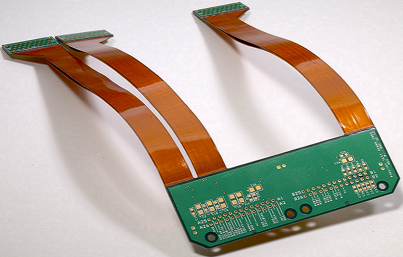
Rigid flex PCB manufacturing integrates rigid FR-4 sections and flexible polyimide circuits into one continuous interconnect structure. The rigid areas support components, connectors, and high-density routing, while the flex areas bend between mechanical sections without separate cables. A reliable service must control the flex material, copper grain direction, bend geometry, coverlay registration, rigid-to-flex transition, lamination pressure, hole plating, impedance, assembly support, and electrical testing. Typical rigid flex products use 4–24 copper layers, 12.5–50 µm polyimide, 18–35 µm flex copper, 0.10–0.25 mm drilled holes, and controlled impedance within ±7% to ±10%.
The manufacturing value is not flexibility alone. A well-designed rigid flex PCB can remove connectors, reduce assembly weight, shorten signal paths, and improve resistance to vibration. These benefits are achieved only when the stack-up, bend area, materials, fabrication process, and assembly method are developed together. The flex circuit is normally created first, then combined with rigid cores and prepreg before final drilling, plating, imaging, routing, inspection, and assembly.
Rigid Flex PCB Manufacturing Service Capabilities
Layer Counts
Rigid flex PCB manufacturing capabilities must be evaluated by complete construction rather than total layer count alone.
Practical production ranges include:
| Capability | Typical Production Range |
|---|---|
| Total copper layers | 4–24 layers |
| Flex copper layers | 1–4 layers |
| Rigid-region thickness | 0.6–3.2 mm |
| Flex-region thickness | 0.08–0.30 mm |
| Minimum rigid trace/space | 50/50–75/75 µm |
| Minimum flex trace/space | 75/75–100/100 µm |
| Mechanical drill | 0.15–0.30 mm |
| Laser microvia | 0.075–0.15 mm |
| Impedance tolerance | ±7% to ±10% |
| Sequential lamination | 1–3 cycles |
A 12-layer rigid flex PCB does not necessarily contain 12 layers through the bend area. A common structure may use 12 copper layers in the rigid sections but only two copper layers through the dynamic flex zone. Reducing the flex layer count lowers bending stress and increases fatigue life.
Production Formats
Service capability may include:
- Rigid flex prototypes from 5–20 pieces
- Engineering builds from 20–100 pieces
- Low-volume production from 100–1,000 pieces
- Panelized SMT assembly
- Selective soldering
- Press-fit connector installation
- Controlled-impedance testing
- Flying probe or fixture-based testing
The quotation must distinguish between:
- Static flex, bent once during installation
- Flex-to-install, bent several times during assembly
- Dynamic flex, bent repeatedly during operation
A static flex section may tolerate a tighter bend radius than a dynamic flex section. Treating both applications as identical can produce copper fatigue or coverlay cracking after deployment.
Materials and Stack-Up
Substrates
Polyimide is the standard flexible PCB substrate because it retains dimensional stability and dielectric performance during bending and soldering.
Typical material values include:
| Material | Typical Thickness |
|---|---|
| Polyimide core | 12.5–50 µm |
| Flexible adhesive | 12.5–50 µm |
| Coverlay polyimide | 12.5–25 µm |
| Rigid FR-4 core | 0.10–1.50 mm |
| Bonding film | 25–100 µm |
Rigid sections commonly use high-Tg FR-4 with a glass-transition temperature of 170°C or higher when the board must survive lead-free assembly near 245°C.
Adhesiveless flex laminate is preferred for thin dynamic structures because it reduces total thickness and avoids an extra adhesive interface. Adhesive-based laminate remains useful for cost-sensitive or static applications, but acrylic adhesive can produce greater Z-axis expansion during thermal processing. Flex construction may begin with adhesive-coated polyimide or an adhesiveless copper-polyimide laminate.
Copper
Copper selection affects flexibility, current capacity, impedance, and fatigue resistance.
The two main options are:
| Copper Type | Main Property | Best Application |
|---|---|---|
| Rolled annealed copper | Elongated grain structure with improved bending fatigue resistance | Dynamic bending and repeated-flex applications |
| Electrodeposited copper | Good circuit definition and lower material cost | Static flex sections and rigid regions |
Typical flex copper thicknesses are:
- 12 µm for ultra-thin circuits
- 18 µm for high-density flex routing
- 35 µm for standard current and durability
- 70 µm for higher current with limited bending
Rolled annealed copper is normally selected when the circuit experiences repeated bending. Traces should run perpendicular to the bend line, and copper grain orientation should be confirmed with the material supplier for severe dynamic applications.
Coverlay and Adhesives
Coverlay protects flex copper in the same general way solder mask protects a rigid PCB, but coverlay is a laminated polyimide film rather than a photoimageable liquid coating.
Typical design allowances include:
- Coverlay opening expansion: 0.10–0.25 mm per side
- Coverlay-to-bend transition clearance: 0.5–1.0 mm
- Adhesive squeeze-out allowance: 0.10–0.30 mm
- Stiffener overlap beyond pad edge: 0.5–1.5 mm
Coverlay registration is less precise than rigid-board solder mask registration. Fine-pitch pads below 0.50 mm may require photoimageable covercoat or larger openings to prevent coverlay from partially covering the pad.
Design and Analysis
Bend and Routing Rules
Bend radius must be based on flex thickness, copper layers, bend frequency, and copper type.
Practical starting points are:
| Flex Construction | Minimum Static Bend Radius | Dynamic Bend Radius |
|---|---|---|
| Single-layer flex | 6× flex thickness | 10× flex thickness or greater |
| Double-layer flex | 10× flex thickness | 20× flex thickness or greater |
| Multilayer flex | 12× flex thickness | 20–30× flex thickness |
For a 0.15 mm two-layer flex section, a static bend radius of approximately 1.5 mm is a practical lower limit. A dynamic application may require 3.0 mm or more.
Bend-zone routing should use:
- Curved traces rather than 90-degree corners
- Staggered conductors on adjacent layers
- Uniform trace widths
- Teardrops at pad transitions
- No plated holes in the active bend
- No abrupt copper-width changes
Rigid-to-Flex Transition
The rigid-to-flex transition is one of the highest-stress regions.
Design controls include:
- Keep vias at least 1.0–2.0 mm from the rigid edge
- Extend coverlay 0.5–1.0 mm into the rigid section
- Avoid component pads within 2.0 mm of the transition
- Use fillets or curved outline corners
- Avoid copper-plane termination directly at the edge
A straight rigid edge can act as a mechanical knife against the flex material. Rounded transitions, controlled adhesive flow, and gradual copper-density changes reduce localized strain.
Impedance and Plane Design
Rigid and flex regions have different dielectric thicknesses and material properties. A 50-ohm trace may therefore require different widths in each region.
Typical values include:
- Single-ended impedance: 50Ω ±7% to ±10%
- Differential impedance: 90Ω or 100Ω ±10%
- Flex dielectric thickness: 25–75 µm
- Controlled flex trace width: 75–150 µm, depending on stack-up
Solid copper planes increase stiffness. Dynamic flex zones often use hatched ground patterns with 30%–60% copper coverage, but the impedance must be modeled because a hatched reference plane changes field distribution.
Fabrication Process
Flex Layer Creation
The flex circuit is manufactured before final rigid-flex lamination.
The process normally follows:
- Prepare polyimide laminate.
- Drill registration and via holes.
- Deposit electroless copper.
- Electroplate the vias.
- Image and etch the copper circuit.
- Apply coverlay.
- Cure and profile the flex subassembly.
Flex holes require additional support because thin polyimide can stretch or distort. Multiple flex panels may be temporarily supported between rigid backup materials during drilling. Flex through-hole copper may be specified near 25 µm to reinforce the hole wall and pad connection.
Surface Preparation and Lamination
Surface preparation creates adhesion between copper, polyimide, bonding films, prepreg, and rigid cores.
Controlled operations include:
- Plasma treatment
- Chemical cleaning
- Copper surface roughening
- Moisture removal
- Lay-up registration
- Lamination pressure and temperature
Typical lamination values depend on the material set, but production commonly uses:
- Temperature: 170–200°C
- Pressure: 1.5–3.5 MPa
- Vacuum-assisted lamination
- Controlled heating and cooling ramps
Excessive pressure can push adhesive into flex cavities or coverlay openings. Insufficient pressure can leave voids at the rigid-to-flex transition.
Drilling, Plating, and Routing
After final lamination, the rigid-flex panel is drilled and plated to connect the rigid and flex layers.
Key controls include:
- Drill registration: commonly ±75 µm
- Finished mechanical hole: 0.20 mm or greater
- Hole-wall copper: 20–25 µm or project-defined
- Laser microvia diameter: 75–150 µm
- Rigid-to-flex depth control: typically ±50–100 µm
The final outline may require:
- CNC routing in rigid areas
- Laser cutting in thin flex areas
- Controlled-depth routing over flex windows
- Mechanical punching for stable high-volume flex profiles
The rigid sections are removed above the flex region without cutting or scoring the flexible circuit. Profiling errors can expose copper, leave glass fibers against the flex, or reduce the intended bend length.
Assembly and Testing
Assembly Process
Rigid flex PCB assembly requires physical support because the flex sections cannot pass unsupported through printing, placement, and reflow.
A typical assembly flow uses:
- Custom carrier fixture
- Vacuum or mechanical board support
- 0.08–0.15 mm stencil
- SPI inspection
- Automated placement
- Lead-free reflow at 235–250°C peak
- AOI and X-ray
- Selective soldering where required
The flex tails should remain flat and protected from direct conveyor contact. A carrier must support the rigid regions without clamping the active bend area.
Quality and Reliability Testing
Quality control should cover fabrication and assembly.
Required inspections may include:
- Microsection analysis
- Coverlay registration check
- Adhesive-flow inspection
- Hole-wall copper measurement
- Continuity and isolation testing
- Impedance coupon testing
- AOI
- X-ray
- Flex cycling
- Thermal stress testing
IPC-2223 defines sectional design requirements for flexible and rigid-flex printed boards. IPC-6013 covers qualification and performance requirements for flexible and rigid-flex boards. IPC-2221 provides generic printed-board design principles, while IPC-A-600 and IPC-A-610 address board and assembly acceptability. Current IPC standards and revision information should be verified through the official standards catalog before the purchase order is released.
Rigid Flex vs Cable Assembly
| Factor | Rigid Flex PCB | PCB With Cable |
|---|---|---|
| Connector count | Lower | Higher |
| Assembly steps | Fewer | More |
| Space requirement | Lower | Higher |
| Initial fabrication cost | Higher | Lower |
| Vibration reliability | Higher when the bend structure is correctly designed | Dependent on connector and cable reliability |
| Design change flexibility | Lower after tooling and stack-up approval | Easier cable replacement or modification |
Rigid flex is most valuable when eliminating two or more connectors reduces weight, size, assembly labor, and potential field failures.
Common Applications
Medical
Medical applications include:
- Portable diagnostic equipment
- Implantable or wearable electronics
- Surgical instruments
- Imaging-system modules
Typical requirements are:
- Compact three-dimensional packaging
- Controlled material traceability
- IPC Class 3 workmanship where specified
- 100% electrical testing
- Repeated bend validation where movement occurs
A rigid flex PCB can replace several connectors inside a handheld instrument, reducing assembly joints while maintaining a thin mechanical profile.
Aerospace and Defense
Aerospace and defense designs use rigid flex circuits in:
- Avionics
- Radar modules
- Guidance systems
- Satellite electronics
- Communication equipment
Typical operating ranges may extend from −55°C to +125°C. Products can also require vibration, thermal shock, humidity, and outgassing control.
Rigid flex designs are useful where connector mass, vibration, and limited enclosure space make cable assemblies less reliable.
Automotive
Automotive applications include:
- Camera modules
- Battery-management systems
- Steering controls
- Infotainment systems
- Lighting modules
Common requirements include:
- −40°C to +125°C operation
- Thermal cycling
- Vibration resistance
- Controlled-impedance communication
- High material and process traceability
Flex sections should not be routed against sharp metal edges or placed under continuous tensile load inside the vehicle assembly.
Consumer Electronics
Consumer electronics use rigid flex PCB technology in:
- Foldable devices
- Cameras
- Wearable products
- Earphones
- Compact computing systems
The primary value is packaging density. Rigid flex can connect multiple planes in a small enclosure while reducing connector height and cable-routing space.
Factory Production Case
Ten-Layer Medical Controller
A medical controller required:
- 10 total copper layers
- Two-layer dynamic flex section
- 1.2 mm rigid thickness
- 0.16 mm flex thickness
- 18 µm rolled annealed flex copper
- 75/75 µm flex trace/space
- 0.20 mm finished holes
- 50Ω impedance at ±10%
- ENIG surface finish
- 500,000 target bend cycles
The first 20-piece pilot build developed intermittent opens after 42,000–78,000 bend cycles.
Root Cause and Correction
Cross-section and mechanical review identified:
- Bend radius of only 1.2 mm
- Two traces aligned directly above each other
- Coverlay termination at the rigid edge
- Copper neck-down inside the bend
The production team changed:
- Bend radius from 1.2 mm to 3.0 mm.
- Trace layers from aligned to staggered.
- Coverlay extension to 0.8 mm inside the rigid area.
- Copper neck-down to a constant 0.10 mm trace.
- Transition corners from square to 1.0 mm radius.
- Flex copper orientation to rolled annealed material.
The revised 40-piece validation lot exceeded 500,000 cycles without electrical opens. First-pass assembly yield increased from 92.5% to 98.8%, and manual flex-tail rework fell from eight assemblies to one.
Common Design Errors
Incorrect Bend Geometry
Production failures often result from:
- Bend radius below 6–10 times flex thickness
- Plated holes inside the bend zone
- Sharp trace corners
- Stacked traces on adjacent layers
- Copper planes across dynamic bends
These conditions concentrate strain and shorten fatigue life.
Incomplete Stack-Up Data
A rigid flex manufacturing package must define:
- Material type
- Copper type and thickness
- Flex and rigid thickness
- Adhesive or adhesiveless construction
- Coverlay thickness
- Bend direction and radius
- Controlled-impedance regions
- Final folded geometry
Supplying one generic stack-up without separate rigid and flex region definitions can lead to incorrect material placement.
Ignoring Assembly Support
A rigid flex PCB may be electrically correct but difficult to assemble when:
- Flex tails interfere with stencil printing
- Components sit too close to bend transitions
- The carrier cannot support the rigid islands
- Tall components prevent fixture clamping
- Flex sections contact the reflow conveyor
Assembly tooling should be reviewed before panel release.
FAQ
What is rigid flex PCB manufacturing?
Answer: Rigid flex PCB manufacturing combines flexible polyimide circuits and rigid FR-4 regions into one laminated board. The process includes flex-layer fabrication, coverlay application, rigid-flex lamination, drilling, plating, imaging, profiling, inspection, and electrical testing.
How many layers can a rigid flex PCB use?
Answer: Common rigid flex boards use 4–24 total copper layers, while the bend area often contains only one or two flex copper layers. Higher layer counts are possible, but added flex layers increase stiffness, thickness, manufacturing cost, and bending stress.
Which materials are used in rigid flex PCB fabrication?
Answer: Typical materials include polyimide flex cores, rolled annealed or electrodeposited copper, polyimide coverlay, acrylic or epoxy adhesive, bonding film, high-Tg FR-4 cores, and rigid-board prepreg. Dynamic flex applications generally favor thin adhesiveless polyimide and rolled annealed copper.
How should a rigid flex PCB manufacturer be selected?
Answer: Selection should be based on demonstrated stack-up capability, flex-material control, coverlay registration, controlled-depth routing, hole plating, impedance testing, flex-cycle validation, PCB assembly support, and experience with the required IPC class. The RFQ should include the unfolded outline, folded model, bend radius, layer structure, materials, test requirements, and annual quantity.

![Understanding PCB Costs & Pricing [Your Complete Guide]](https://hdicircuitboard.com/wp-content/uploads/elementor/thumbs/Understanding-PCB-Costs-Pricing-Your-Complete-Guide-qzzhe6mcaxuolkux3xalfktgavumi9y1aqfbs9bpv4.webp "Understanding PCB Costs & Pricing [Your Complete Guide]")