







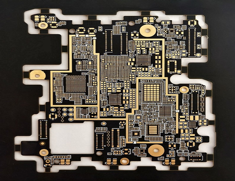
An HDI PCB is a high density interconnect printed circuit board that uses microvias, blind and buried vias, fine conductor geometry, thin dielectric layers, via-in-pad, and sequential build-up structures to route more electrical connections in less board area. Successful HDI PCB design is not simply a matter of shrinking traces and vias. Stack-up, microvia aspect ratio, BGA pitch, impedance, copper thickness, lamination sequence, annular-ring allowance, assembly limits, and the HDI PCB manufacturer’s qualified process must be defined together before detailed routing begins. HDI technology commonly supports 0.35–0.50 mm pitch BGAs, 50–100 μm microvias, 50/50–100/100 μm line and space, and one to three build-up levels, while ultra-HDI moves below approximately 50 μm conductor geometries and often requires semi-additive processing.
IPC-2221 provides general printed board design requirements, while IPC-2226 specifically addresses HDI structures and microvia-based designs. IPC-6012 defines qualification and performance requirements for rigid printed boards. Material requirements may also involve IPC-4101 or IPC-4104 depending on the dielectric technology selected. HDI design guidance consistently emphasizes planning the stack-up and microvia architecture before routing because fabrication capability ultimately limits usable feature size.
What’s HDI?
High Density Interconnect Basics
High density interconnect increases routing density by replacing large mechanically drilled through vias with smaller blind, buried, and laser-drilled connections.
Typical HDI features include:
- Laser microvias: 60–125 μm
- Blind and buried vias
- 50–100 μm conductor widths
- Via-in-pad structures
- Thin build-up dielectrics: 40–100 μm
- Sequential lamination
- Fine-pitch components down to approximately 0.20–0.50 mm pitch
The main engineering value is not only a smaller PCB. Shorter interconnections reduce via stubs, decrease parasitic inductance, and create more routing channels beneath dense BGAs. HDI therefore supports smartphones, AI modules, networking equipment, medical electronics, automotive controllers, and semiconductor test hardware. Current industry design guidance identifies microvias, blind and buried vias, fine lines, via-in-pad, and sequential build-up as defining HDI features.
Microvias
Microvia Geometry
Microvias are usually laser-drilled interconnections between adjacent or nearby layers.
Typical production dimensions are:
| Parameter | Typical HDI Range |
|---|---|
| Laser via diameter | 60–125 μm |
| Common production diameter | 75–100 μm |
| Capture pad | 180–275 μm |
| Dielectric depth | 50–100 μm |
| Preferred aspect ratio | 0.75:1–1:1 |
| Copper-fill dimple | <15–25 μm |
A 75 μm microvia drilled through a 60 μm dielectric has an aspect ratio of 0.8:1, which provides substantially better plating access than a 75 μm microvia through a 125 μm dielectric.
Microvia aspect ratio directly influences reliability because deeper, narrower holes are harder to clean and plate uniformly. Industry HDI guidance generally favors aspect ratios below 1:1 for robust production.
Blind and Buried Vias
Blind Via Structure
A blind via connects an external layer to an internal layer without passing through the entire board.
Examples include:
- L1–L2 laser microvia
- L1–L3 stacked microvias
- L12–L11 bottom-side microvia
- Mechanically drilled L1–L4 blind via
Typical mechanical blind-via diameter:
- 0.15–0.30 mm
Laser blind vias are much smaller and are normally used in HDI build-up layers.
Buried Via Structure
A buried via connects internal layers only and disappears after final lamination.
Examples:
- L3–L8 buried via in a 2+6+2 stack
- L2–L7 buried via in a 1+6+1 stack
Buried vias require drilling, plating, imaging, testing, and lamination before the outer structure is completed, which increases manufacturing stages and cost.
Fine Lines and Spaces
Fine lines increase the number of routing channels available between pads.
Typical production levels are:
| Technology | Typical Line / Space |
|---|---|
| Conventional multilayer | 100/100 μm |
| Standard HDI | 75/75 μm |
| Advanced HDI | 50/50–60/60 μm |
| Ultra-HDI | <50/50 μm |
Starting copper thickness is critical. A 9–12 μm foil can be etched into 50–75 μm conductors more predictably than 35 μm copper because lateral undercut is lower.
Designing 50/50 μm geometry merely because a supplier lists it as a minimum capability does not mean it is suitable for every production panel. Manufacturing yield, panel size, copper weight, and annual volume must also be considered.
Sequential Build-Up
SBU Manufacturing Logic
Sequential Build-Up, or SBU, forms HDI layers around a conventional core through repeated lamination and microvia processing.
A typical sequence is:
- Fabricate the central core.
- Drill and plate buried vias.
- Laminate a thin dielectric and copper layer.
- Laser drill microvias.
- Desmear and metallize.
- Copper fill the microvias.
- Image and etch the new conductor layer.
- Repeat for additional build-up levels.
Sequential lamination is fundamental to HDI because thin dielectric layers are added around a thicker core in separate process cycles.
HDI PCB Stack-Up Types
1+N+1
A 1+N+1 stack-up has:
- One build-up layer on the top
- N conventional core layers
- One build-up layer on the bottom
Examples:
- 1+4+1 = 6 layers
- 1+6+1 = 8 layers
This structure supports one laser microvia level per side and offers lower manufacturing complexity than multi-level HDI.
i+N+i
The notation i+N+i indicates multiple symmetrical build-up levels.
Examples:
- 2+4+2 = 8 layers
- 2+6+2 = 10 layers
- 3+8+3 = 14 layers
Each additional build-up level adds lamination, laser drilling, metallization, filling, imaging, and inspection.
Any Layer HDI
Any Layer HDI, often described as Every Layer Interconnect, allows laser microvias between adjacent layers throughout the PCB.
Its main advantages are:
- Maximum routing freedom
- Short vertical transitions
- High via-in-pad density
- Reduced reliance on through holes
The manufacturing cost is higher because many or all copper layers require repeated laser drilling, copper filling, and precise registration.
HDI Stack-Up Planning
Notation and Symmetry
Stack-up planning should be completed before routing begins.
A production stack should define:
- Layer count
- Copper thickness
- Core and prepreg thickness
- Build-up dielectric thickness
- Via span
- Lamination sequence
- Controlled impedance
Mechanical symmetry is preferred because equal build-up layers and balanced copper reduce bow and twist.
A 2+6+2 structure is generally mechanically easier to control than 2+6+1 because both sides see more similar thermal and resin stresses.
Reference Planes
High-speed traces should remain adjacent to continuous reference planes.
Typical targets include:
- 50 Ω single-ended
- 85 Ω PCIe differential
- 90 Ω USB differential
- 100 Ω Ethernet or general differential
Build-up dielectric thicknesses of 50–80 μm often require trace widths between approximately 60 and 120 μm depending on copper thickness and Dk.
Via and Pad Strategies
Via-in-Pad
Via-in-Pad places the microvia inside the BGA or component pad.
A typical 0.40 mm pitch design may use:
- 75 μm microvia
- 200 μm pad
- Copper-filled via
- Planarized surface
- ENIG or ENEPIG finish
The via must be filled and planarized when soldering directly over it. An unfilled opening can wick solder away from the joint.
Stacked vs. Staggered
| Factor | Stacked Microvia | Staggered Microvia |
|---|---|---|
| Density | Highest | Lower |
| Footprint | Smallest | Larger |
| Registration demand | Highest | Moderate |
| Thermal stress | Concentrated | Distributed |
| Filling requirement | Critical | Less demanding |
| Cost | Higher | Lower |
| Reliability margin | Lower if poorly controlled | Generally wider |
Stacked microvias are justified when BGA escape density requires vertical alignment. Staggered structures are preferred where routing space permits because they distribute stress and reduce alignment sensitivity.
Routing and Signal Integrity
Trace Widths and Spacing
Typical routing values include:
- General HDI: 75/75 μm
- Dense BGA regions: 60/60 μm
- Advanced HDI: 50/50 μm
- Ultra-HDI: below 50/50 μm
Fine lines should not be used throughout the entire PCB simply because they are required under one processor. Wider geometry elsewhere improves yield and reduces copper resistance.
Controlled Impedance
Impedance calculations must use:
- Finished copper thickness
- Pressed dielectric thickness
- Actual Dk
- Copper roughness
- Solder mask
- Reference-plane distance
External copper may grow by 15–25 μm during plating. Modeling an 18 μm foil while the final conductor is 35–40 μm can cause several ohms of impedance error.
Short Signal Paths
HDI reduces unnecessary vertical transitions and through-via stubs.
High-speed routing should:
- Use continuous reference planes
- Minimize layer changes
- Add return vias beside signal vias
- Avoid plane splits
- Keep differential spacing consistent
- Remove unused through-hole stubs where required
The electrical value of HDI is therefore not only density; shorter interconnect geometry can also improve signal performance.
Best Practices for Manufacturing
Early Fabricator Engagement
The HDI PCB manufacturer should be involved before routing is finalized.
Confirm:
- Minimum line/space
- Laser via diameter
- Minimum pad diameter
- Microvia aspect ratio
- Stacked-via limit
- Copper-fill capability
- Lamination count
- Material availability
- Impedance capability
Industry HDI design guidance specifically emphasizes contacting the fabricator early because BGA pitch, via size, dielectric thickness, and process limits jointly determine manufacturability.
Annular Rings
A 75 μm microvia inside a 200 μm pad leaves:
- 62.5 μm nominal radial copper
If laser registration tolerance is ±25 μm, worst-case remaining capture can decrease to approximately 37.5 μm before etching tolerance is considered.
Aggressive pad reduction therefore creates a much smaller manufacturing margin than nominal geometry suggests.
Strict DRC
HDI design rules should separately define:
- Microvia-to-trace clearance
- Capture pad diameter
- Microvia aspect ratio
- Stacked-via count
- Fine-line regions
- Via-in-pad locations
- Impedance widths
- Solder mask expansion
Rules-driven design is particularly important in HDI because DFM limits vary significantly with process and materials.
Ultra-HDI PCB Design
Ultra-HDI Specifications
Ultra-HDI generally pushes beyond conventional HDI feature sizes.
Common industry thresholds include one or more of the following:
| Feature | Conventional HDI | Ultra-HDI |
|---|---|---|
| Line width | 50–100 μm | <50 μm |
| Spacing | 50–100 μm | <50 μm |
| Microvia diameter | 75–125 μm | <75 μm |
| Dielectric thickness | 50–100 μm | <50 μm |
| Fabrication method | Subtractive | mSAP/SAP increasingly used |
Current industry descriptions commonly classify ultra-HDI by conductor width or spacing below roughly 50 μm and by similarly aggressive via or dielectric dimensions.
Structure Type
Ultra-HDI structures may use:
- Any-layer microvias
- Very thin dielectric films
- Embedded traces
- mSAP
- SAP
- Substrate-like processing
Subtractive etching becomes increasingly difficult as conductor dimensions approach 25–40 μm because lateral etching consumes a large percentage of the conductor width.
Ultra-HDI Design Considerations
Manufacturing Limits vs. Production Reality
A fabricator may demonstrate 35/35 μm capability on a development coupon but qualify 50/50 μm for production.
The difference reflects:
- Panel size
- Copper uniformity
- Imaging stability
- Etching distribution
- Registration
- Lot-to-lot repeatability
Engineering releases should use production capability rather than laboratory minimum capability.
Advanced Material Selection
Ultra-HDI materials require:
- Thin stable dielectrics
- Low-profile copper
- Good copper adhesion
- Controlled dimensional movement
- Reliable laser interaction
HDI material selection must also survive multiple thermal cycles and repeated sequential lamination. HDI design sources emphasize dielectric adhesion, thermal compatibility, plated-microvia reliability, and stable spacing as key material criteria.
Impedance and Signal Integrity
At 25–50 μm conductor widths, a 5 μm dimensional change can represent a 10–20% geometry variation.
Ultra-HDI impedance design therefore requires tighter control of:
- Copper thickness
- Trace width
- Dielectric thickness
- Etch profile
- Copper roughness
- Reference plane geometry
Solder Mask and Assembly Constraints
Fabrication geometry can become smaller than assembly capability.
Typical concerns include:
- Solder mask dams below 50–75 μm
- 0.30–0.40 mm pitch BGA
- Paste aperture alignment
- Via-in-pad coplanarity
- BGA X-ray inspection
- Microvia fill dimple
A PCB that can be fabricated at 35/35 μm may still be difficult to assemble if solder mask and stencil processes cannot maintain comparable registration.
Inspection and Testing Strategy
Quality control for HDI circuit boards should include inspections throughout the build sequence.
Typical controls are:
| Process | Inspection | Typical Target |
|---|---|---|
| Inner-layer imaging | AOI | No opens or shorts |
| Laser drilling | Optical measurement | ±10–25 μm diameter/position |
| Microvia cleaning | Microsection | No target residue |
| Copper filling | X-ray / microsection | No rejectable void |
| Lamination | Registration coupon | ±25–50 μm |
| Fine-line etching | AOI | ±10–15 μm width |
| Impedance | TDR coupon | ±7% to ±10% |
| Final electrical test | Fixture / flying probe | 100% nets |
Microsections should verify:
- Via-bottom copper
- Knee plating
- Fill profile
- Target-pad erosion
- Dielectric thickness
- Registration
- Interlayer separation
Thermal-cycle or interconnect stress testing becomes increasingly important for stacked microvias because the vertical interfaces experience repeated expansion stress.
Factory Case Study
16-Layer AI Processing Board
A factory produced a 16-layer high density interconnect PCB with:
- 3+10+3 stack-up
- 0.40 mm pitch BGA
- 75 μm microvias
- 200 μm microvia pads
- 75/75 μm general routing
- 60/60 μm BGA escape routing
- 50 Ω single-ended impedance
- 100 Ω differential impedance
- 1.8 mm finished thickness
- ENIG surface finish
Initial Production Problems
The first engineering build showed:
- Build-up registration shift: 52 μm
- Stacked-microvia void rate: 5.9%
- Differential impedance deviation: +10.8%
- Fine-line open rate: 4.2%
- First-pass panel yield: 89.4%
Failure analysis identified:
- Three stacked microvia levels were used across the entire BGA region.
- Finished outer copper exceeded the impedance model by 9 μm.
- One artwork compensation factor was used for all lamination cycles.
- Edge-panel etching removed more copper than center-panel etching.
- Microvia dimple averaged 27 μm before the next build-up.
Corrective Actions
The revised structure used:
- Staggered microvias outside the critical processor core
- Two stacked levels only where routing density required them
- Separate X-Y compensation for each SBU layer
- Finished copper values in the field-solver model
- Edge-specific etch compensation of 8–10 μm
- Copper-fill profile adjustment
- Dimple control below 12 μm
- Microsections at panel center and four edge positions
Measured Improvement
| Result | Initial Build | Revised Build |
|---|---|---|
| Registration shift | 52 μm | 23 μm |
| Microvia void rate | 5.9% | 0.6% |
| Impedance deviation | +10.8% | ±5.7% |
| Fine-line opens | 4.2% | 0.4% |
| First-pass yield | 89.4% | 98.3% |
The largest improvement came from reducing unnecessary stacked-via usage and treating every build-up layer as a separate dimensional process rather than applying one global compensation factor.
Common Design Errors
Stack-Up Defined After Routing
Routing before stack-up approval can create:
- Unbuildable microvia depth
- Wrong impedance geometry
- Excessive lamination count
- Asymmetric structures
Microvia Aspect Ratio Too High
A 75 μm microvia through a 100 μm dielectric produces a 1.33:1 ratio. A 100 μm hole through a 75 μm dielectric produces a more robust 0.75:1 structure.
Stacked Microvias Everywhere
Stacked microvias should be reserved for density-critical locations. Using them globally increases fill complexity, thermal stress, inspection burden, and fabrication cost.
Ignoring Finished Copper
Impedance calculations based only on starting foil thickness often produce lower-than-target impedance after plating.
DRC Based on Absolute Minimums
A minimum 50/50 μm capability does not mean every trace on a production board should use 50/50 μm. Use the largest geometry that routing permits.
FAQ
What Is an HDI PCB?
Question: What makes an HDI PCB different from a conventional multilayer PCB?
Answer: An HDI PCB uses laser microvias, blind and buried vias, fine lines, thin dielectrics, via-in-pad, and sequential build-up technology to increase routing density. These features support fine-pitch BGAs and shorter electrical interconnections.
What Does 2+6+2 Mean?
Question: What does i+N+i notation mean in HDI PCB design?
Answer: The first and last numbers represent sequential build-up layers, while N represents the conventional central core. A 2+6+2 HDI PCB has two build-up layers on each side of a six-layer core, giving ten copper layers in total.
Are Stacked or Staggered Microvias Better?
Question: Which microvia structure provides better reliability?
Answer: Stacked microvias provide maximum routing density but require very accurate filling, planarization, and registration. Staggered microvias consume more space but normally provide a wider manufacturing and thermal reliability margin.
What Is Ultra-HDI PCB Design?
Question: When does an HDI design become ultra-HDI?
Answer: Ultra-HDI commonly describes PCB structures with conductor width or spacing below approximately 50 μm, microvias below roughly 75 μm, very thin dielectrics, or substrate-like processing such as mSAP or SAP. Production feasibility depends heavily on the manufacturer’s qualified process rather than a single universal dimensional threshold.

![Understanding PCB Costs & Pricing [Your Complete Guide]](https://hdicircuitboard.com/wp-content/uploads/elementor/thumbs/Understanding-PCB-Costs-Pricing-Your-Complete-Guide-qzzhe6mcaxuolkux3xalfktgavumi9y1aqfbs9bpv4.webp "Understanding PCB Costs & Pricing [Your Complete Guide]")