
The Cost of Overlooking Impedance Issues in HDI Design
HDI printed circuit boards push the limits of miniaturization, but their dense layouts and fine features make impedance control exponentially challenging. As an HDI board engineer or procurement specialist, you’ve likely faced:
- 10-15% yield loss due to unforeseen impedance mismatches in 12+ layer HDI designs
- Field failures from signal reflections caused by microvia-induced impedance spikes
- Failed IPC-6012 Class 3 qualification because of inconsistent dielectric thickness
- Delays from reworking differential pairs that deviated 8-10Ω from target values
- Escalated costs from using premium materials without addressing root impedance issues
These problems aren’t just technical nuisances—they translate to missed deadlines, wasted resources, and compromised product reliability. This guide delivers factory-proven solutions tailored to the unique challenges of high density interconnect PCBs.
Learn more about :HDI PCB Impedance Control: Design, Manufacturing & Performance Guide
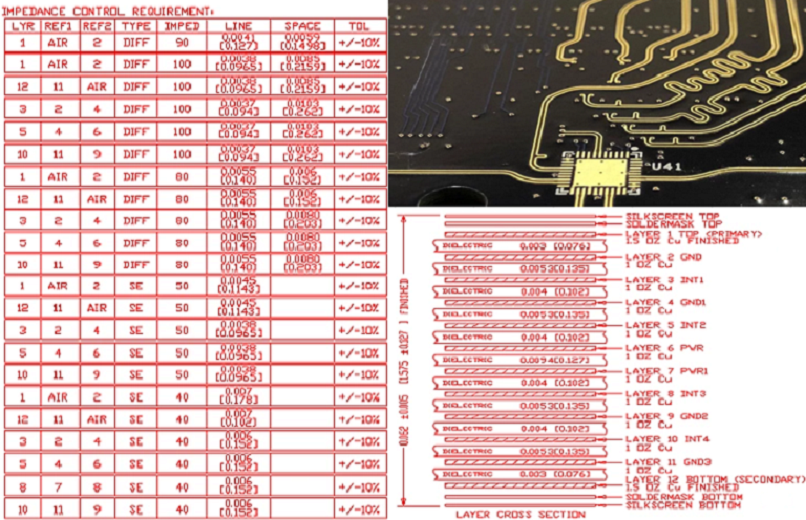
Core Technical Principles & Parameters
Common Controlled Impedance Issues in HDI PCBs
Common Impedance Disturbances
- Trace Geometry Inconsistencies
- Narrowed traces (3mil vs. specified 4mil) increase impedance by 8-10Ω
- Unequal differential pair spacing (5mil vs. 6mil) causes 5-7Ω mismatch
- Trapezoidal etch profiles reduce effective trace width, lowering impedance by 3-4Ω
- Reference Plane Deficiencies
- Split ground planes create 10-15% impedance spikes in affected areas
- Inadequate plane clearance (less than 3x trace width) disrupts return paths
- Voids from clustered microvias break continuous reference planes
- Solder Mask Effects
- Uncompensated solder mask (0.5-1mil thickness) reduces microstrip impedance by 2-3Ω
- Uneven mask application causes inconsistent impedance across the board
Material-Related Issues
- Dielectric Constant (Dk) Variations
- Generic FR4 Dk values (4.0) vs. frequency-specific values (3.8 at 10GHz) cause 3-5Ω errors
- Resin content fluctuations (±5%) in HDI laminates alter Dk by 0.1-0.3
- Moisture absorption increases Dk, lowering impedance by 4-6Ω
- Copper-Related Anomalies
- Copper roughness (1-3μm) increases insertion loss and modifies impedance
- Thickness variations (0.5oz vs. 1oz) create 5-7Ω differences
- Plating inconsistencies at microvia sites introduce local impedance shifts
Manufacturing Issues
- Etching Variability
- Over-etching reduces trace width by 0.3-0.5mil, increasing impedance by 6-8Ω
- Under-etching has the opposite effect, lowering impedance by 4-5Ω
- Etch factor deviations (1.5 vs. target 2.0) create non-uniform trace profiles
- Lamination Imperfections
- Dielectric thickness variation (±0.2mil) shifts impedance by 2-3Ω
- Prepreg flow during lamination reduces dielectric height, lowering impedance
- Layer misalignment (≥0.5mil) disrupts stripline symmetry
- Via Parasitics
- Unbackdrilled via stubs act as resonant structures, causing 3-4Ω impedance spikes
- Microvia diameter variations (6mil vs. 8mil) introduce inductance differences
Design and Layout Issues
- Differential Pair Mismanagement
- Length mismatch (>5mil) causes delay skew and impedance degradation
- Components or vias between differential pairs create discontinuities
- Asymmetrical routing breaks impedance symmetry
- Layer Transition Problems
- Signal layer changes without stitching vias disrupt return paths
- Different reference planes on adjacent layers create 7-9Ω impedance jumps
- Via clusters near signal traces introduce parasitic capacitance
- Crosstalk-Induced Impedance Shifts
- Inadequate trace spacing (less than 3W) couples signals, altering impedance
- High-density routing increases mutual inductance between adjacent traces
Learn more about : How to Calculate Impedance for HDI Boards
How to Fix Controlled Impedance Issues in HDI PCBs
Correct Trace Geometry Problems
- Precision Adjustments
- Widen narrow traces by 0.2-0.3mil per 1Ω needed to lower impedance
- Maintain consistent differential pair spacing (±0.1mil) using design rules
- Compensate for etch taper by specifying target finished trace width
- Length Matching Techniques
- Implement serpentine routing on shorter differential pair traces (minimum 15mil pitch)
- Place serpentines near mismatch sources (within 100mil of vias or bends)
- Keep total length mismatch below 2% of signal wavelength
Resolve Dielectric & Material Issues
- Dielectric Control
- Use frequency-specific Dk values (e.g., 3.8 for FR4 at 10GHz, 3.2 for high-speed laminates)
- Specify dielectric thickness tolerance of ±0.1mil for HDI designs
- Pre-bake laminates to remove moisture (120°C for 4 hours)
- Material Selection
- Choose low-loss materials (Df ≤0.005) for signals above 10Gbps
- Select laminates with consistent resin content (±2%)
- Use smooth copper (Ra ≤0.8μm) for high-frequency HDI circuits
Fix Reference Plane & Layout Issues
- Reference Plane Optimization
- Eliminate split planes under controlled impedance traces
- Maintain 3W clearance between traces and plane edges
- Add stitching capacitors (10nF-100nF) when crossing reference planes
- Crosstalk Mitigation
- Follow 3W rule for adjacent traces (5W for clock signals)
- Maintain 30mil keep-out from other signals for differential pairs
- Increase spacing to 50mil for periodic signals to reduce interference
Mitigate Via & Microvia Parasitics
- Via Optimization
- Implement backdrilling to remove unused via stubs (reduces inductance by 0.3nH)
- Use blind/buried microvias (6-8mil diameter) instead of through-hole vias
- Stagger via clusters to maintain reference plane continuity
- Transition Compensation
- Narrow traces by 0.2mil before/after vias to offset parasitic capacitance
- Place stitching vias within 50mil of signal vias
- Use symmetric anti-pad sizes (1.5x via diameter)
Improve Manufacturing & Quality Control
- Process Validation
- Simulate manufacturing tolerances (±0.5mil trace width, ±0.2mil dielectric)
- Incorporate impedance test coupons on every production panel
- Perform TDR testing per IPC-6012 (100% testing for Class 3 HDI)
- Quality Gates
- Microsection coupons to verify dielectric thickness (±0.1mil)
- Monitor etch factor (1.5-2.0) during production
- Implement statistical process control for trace width (CPK ≥1.33)
Key Comparisons for HDI Impedance Control
Microstrip vs. Stripline Impedance Fixes
| Aspect | Microstrip (Outer Layers) | Stripline (Inner Layers) |
|---|---|---|
| Common Issues | Solder mask effects, Dk variation from air | Layer misalignment, dielectric thickness variation |
| Fix Techniques | Compensate for mask thickness, use conformal coating | Ensure symmetric dielectric thickness, tighter lamination control |
| Typical Adjustment | ±0.3mil trace width per 1Ω correction | ±0.2mil dielectric thickness per 1Ω correction |
| Tolerance Target | ±5Ω (IPC-6012 Class 2), ±3Ω (Class 3) | ±4Ω (IPC-6012 Class 2), ±2Ω (Class 3) |
Single-Ended vs. Differential Impedance Solutions
| Aspect | Single-Ended (50Ω/75Ω) | Differential (90Ω/100Ω) |
|---|---|---|
| Primary Issues | Reference plane breaks, trace width variation | Spacing inconsistency, length mismatch |
| Fix Priority | Maintain continuous ground plane | Symmetric routing, length matching |
| Manufacturing Control | Trace width (±0.2mil) | Spacing (±0.1mil), length (±2mil) |
| Test Methodology | Single-ended TDR probe | Differential TDR probe |
HDI Board Factory Case Study
16-Layer HDI for 25Gbps Data Center Application
Project Specifications
- Layer count: 16-layer high density interconnect PCB
- Impedance targets: 50Ω single-ended (±3Ω), 100Ω differential (±5Ω)
- Stack-up: 4 signal layers, 2 power planes, 10 ground planes
- Trace geometry: 4mil width/6mil spacing (differential), 4.2mil width (single-ended)
- Materials: FR4 (Dk=3.8, Df=0.004), 4mil core, 2mil prepreg
- Microvias: 8mil diameter, 1:1 aspect ratio, blind/buried structure
Issues Encountered
- Initial impedance testing revealed stripline differential pairs at 92Ω (8Ω below target)
- Root cause: Dielectric thickness underspecified by 0.5mil due to prepreg flow
- Microvia clusters caused 4-5Ω impedance spikes in critical signal paths
- Outer-layer microstrip traces showed 3-4Ω variation due to uneven solder mask
- Crosstalk between adjacent differential pairs exceeded -30dB at 25GHz
Implemented Fixes
- Adjusted trace width from 4mil to 3.8mil (field solver-optimized)
- Added backdrilling to remove 12mil via stubs
- Compensated solder mask thickness (0.8mil) in impedance calculations
- Increased differential pair spacing from 6mil to 7mil
- Added stitching vias (10mil diameter) every 50mil around microvia clusters
- Implemented 3W spacing rule between all signal traces
Results
- Final impedance: 99.7Ω differential (±1.2Ω), 50.2Ω single-ended (±0.8Ω)
- Crosstalk reduced to -35dB at 25GHz
- Yield improved from 78% to 92%
- Successfully passed IPC-6012 Class 3 qualification
- Signal integrity verified with eye diagram testing (BER <1e-12)
Common Design Errors (Production Perspective)
- Ignoring Microvia Parasitics – Failing to compensate for inductance from microvias (0.1nH each) creates unforeseen impedance spikes. Production fix requires trace width adjustment near vias, adding 1-2 days to rework.
- Overlooking Solder Mask Impact – Assuming solder mask doesn’t affect impedance leads to 2-3Ω deviations. Factories often discover this too late, requiring costly panel rework.
- Generic Dk Values – Using standard FR4 Dk=4.0 instead of frequency-specific values (3.8 at 10GHz) causes systematic impedance errors. This requires material substitution or trace redesign.
- Inadequate Test Coupons – Designing coupons that don’t match HDI stack-up leads to inaccurate impedance measurements. Production teams need to create custom coupons, delaying testing.
- Poor Reference Plane Design – Split planes or insufficient clearance disrupt return paths. Fixing this requires redesigning layer stack-up, adding 1-2 weeks to production.
- Uncontrolled Differential Pair Routing – Asymmetrical paths or length mismatch (>5mil) degrades impedance. Reworking these pairs increases labor costs by 30-40%.
FAQ
- How do HDI PCB impedance issues differ from standard PCB issues?HDI’s fine traces (3-6mil), thin dielectrics (2-4mil), and microvias amplify impedance sensitivity to manufacturing variations, requiring tighter tolerances (±3Ω vs. ±5Ω for standard PCBs) and specialized fixes.
- What is the most cost-effective fix for HDI impedance deviations?Adjusting trace width (±0.2mil per 1Ω correction) is typically 30-40% cheaper than material changes or layer stack-up redesign, with minimal production delays when caught early.
- How can I prevent impedance issues in HDI design before production?Use frequency-specific Dk values, simulate with 2D/3D field solvers that model microvias, incorporate test coupons matching the HDI stack-up, and specify ±0.1mil dielectric thickness tolerance.
- What IPC standards govern HDI impedance control, and what do they require?IPC-2221 specifies impedance design requirements, while IPC-6012 mandates testing methods (TDR) and tolerances (±10% for Class 2, ±5% for Class 3). Both standards require documentation of stack-up, materials, and test results.
If you need HDI PCB with impedance control,contact our engineering team for a free DFM check.


![Understanding PCB Costs & Pricing [Your Complete Guide]](https://hdicircuitboard.com/wp-content/uploads/elementor/thumbs/Understanding-PCB-Costs-Pricing-Your-Complete-Guide-qzzhe6mcaxuolkux3xalfktgavumi9y1aqfbs9bpv4.webp "Understanding PCB Costs & Pricing [Your Complete Guide]")


