What Are the Cost Differences Between 1+N+1, 2+N+2, and Any-Layer HDI PCBs?
High density interconnect (HDI) PCBs are categorized by their stack-up structure, with 1+N+1, 2+N+2, and any-layer designs representing distinct complexity tiers. Each configuration differs in manufacturing processes, material requirements, and performance capabilities, leading to significant cost disparities. This analysis breaks down the cost drivers, technical specifications, and practical applications of each type, adhering to industry standards including IPC-2226 and IPC-6012. For electronic engineers, PCB procurement teams, and electronics enthusiasts, this guide clarifies how design choices impact bottom-line costs while balancing functionality and manufacturability.
Learn more about: What is a HDI Microvia PCB
1+N+1 HDI PCB Stackup
The 1+N+1 configuration is the entry-level HDI solution, defined by one build-up layer on each side of a central core (N layers). It balances basic high-density needs with cost efficiency, making it the most accessible HDI option for volume production.
Cost Baseline & Key Metrics
- Cost position: Lowest among HDI types, typically 10–15% more expensive than conventional multi-layer PCBs.
- Volume pricing: Scales efficiently for production runs of 1,000 units or more, with per-unit cost decreasing by 20–25% compared to small-batch prototyping orders.
- Cost stability: Minimal price fluctuation due to simplified processes and widely available standard materials.
Process & Technical Specifications
- Fabricate the central core (N layers) using conventional lamination and mechanical drilling.
- Perform a single Sequential Lamination cycle to add one build-up layer to each side of the core.
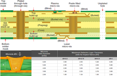
- Laser-drill microvias from 100μm to 125μm, following IPC-2226 aspect ratio requirements of 0.8:1 or lower.
- Apply standard plating and surface finishes including ENIG and HASL.
- Key constraints: No stacked vias; minimum trace and space at 3mil (75μm).
Use Case & Practical Applications
- Mid-range consumer electronics, basic IoT devices, and non-implantable medical tools.
- Supports 0.4mm pitch BGAs and replaces conventional multilayer boards with fewer layers.
2+N+2 HDI PCB Stackup
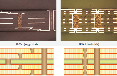
The 2+N+2 configuration adds a second build-up layer on each side of the core, enabling stacked or staggered microvias and improved Signal Integrity.
Cost Premium & Comparative Analysis
- Cost position: 25–40% more expensive than 1+N+1 HDI and 40–60% higher than conventional PCBs.
- Cost breakdown: Additional Sequential Lamination, stacked microvia filling, and tighter alignment controls.
- Value proposition: Reduces required layer count by 20–30% for equivalent routing density.
Process & Technical Specifications
- Two Sequential Lamination cycles per structure.
- Microvias from 75μm to 100μm with copper filling per IPC-6016.
- Laser direct imaging (LDI) for 2–3mil trace and space.
- Supports via-in-pad (VIP) and controlled impedance within ±8–10%.
Use Case & Practical Applications
- Flagship consumer electronics, automotive ADAS, 5G access devices, and high-speed industrial controls.
- Supports 0.3mm pitch BGAs and high-speed memory interfaces.
Any-Layer HDI PCB
Any-layer HDI, also known as Every-Layer Interconnect (ELIC), uses full build-up construction with unrestricted layer-to-layer interconnection.
Cost Premium & Comparative Analysis
- Cost position: 50–80% more expensive than 2+N+2 HDI and 2–3 times the cost of conventional PCBs.
- Cost drivers: Multiple lamination cycles, ultra-fine laser drilling, copper-filled vias, and lower production yields.
- Volume sensitivity: Minimal cost reduction at scale due to inherent structural complexity.
Process & Technical Specifications
- Full build-up without a rigid core, using 3–4 Sequential Lamination cycles.
- Microvias from 50μm to 75μm with alignment accuracy within ±20μm.
- Semi-additive processing (SAP) for 1–2mil trace and space.
- Full compliance with IPC-6012 Class 3 for high-reliability applications.
Use Case & Practical Applications
- Premium smartphones, AI accelerators, high-frequency radar, implantable medical devices, and aerospace electronics.
- Supports 0.2mm pitch BGAs and high-speed signaling above 25Gbps.
Key Cost Drivers Across HDI Configurations
Sequential Lamination Cycles
- 1+N+1: 1 cycle
- 2+N+2: 2 cycles
- Any-layer: 3–4 cycles
Each additional cycle increases base cost by 15–20%.
Microvia Count & Size
- 1+N+1: 100–150 per square inch, 100–125μm
- 2+N+2: 200–300 per square inch, 75–100μm
- Any-layer: 300–500 per square inch, 50–75μm
Smaller microvias increase drilling cost significantly.
Yield Impact
- 1+N+1: 85–95%
- 2+N+2: 80–90%
- Any-layer: 70–85%
A 10% yield drop increases per-unit cost by 15–20%.
Material Requirements
| Material Aspect | 1+N+1 HDI | 2+N+2 HDI | Any-Layer HDI |
|---|---|---|---|
| Core Material | Standard FR-4 (Tg ≥130°C) | High-Tg FR-4 (Tg ≥170°C) | Low-loss high-frequency laminates |
| Dielectric | Standard prepreg (0.1–0.2mm) | Thin prepreg (0.08–0.1mm) | Ultra-thin dielectric (0.04–0.08mm) |
| Copper Foil | Standard electrolytic (1oz) | Low-profile electrolytic (0.5oz) | Reverse-treated ultra-fine foil |
| Surface Finish | HASL, ENIG | ENIG, immersion silver | ENIG, soft gold, or hard gold |
| Relative Material Cost | Baseline | 1.3–1.5x | 2.0–3.0x |
Comparative Cost & Performance Framework
| Parameter | 1+N+1 HDI | 2+N+2 HDI | Any-Layer HDI |
|---|---|---|---|
| Cost vs. Conventional PCB | +10–15% | +40–60% | +100–200% |
| Cost vs. 1+N+1 HDI | Baseline | +25–40% | +50–80% |
| Sequential Lamination Cycles | 1 | 2 | 3–4 |
| Microvia Diameter | 100–125μm | 75–100μm | 50–75μm |
| Trace/Space Minimum | 3mil (75μm) | 2–3mil (50–75μm) | 1–2mil (25–50μm) |
| Production Yield | 85–95% | 80–90% | 70–85% |
| Minimum Supported BGA Pitch | 0.4mm | 0.3mm | 0.2mm |
| Industry Standards | IPC-2226, IPC-6012 Class 2 | IPC-2226, IPC-6016 | IPC-2226, IPC-6012 Class 3 |
| Typical Layer Range | 4–8 | 6–12 | 8–20 |
Long-Tail Considerations & FAQ
When to Select a Higher-Cost HDI Structure
- Upgrade to 2+N+2 if BGA pitch ≤ 0.35mm, frequency ≥ 5GHz, or layer count reduction ≥ 20%.
- Upgrade to any-layer if BGA pitch ≤ 0.25mm, signaling speed ≥ 25Gbps, or form factor is strictly constrained.
PCB vs. PCA: Assembly Cost Impacts
- 1+N+1: Standard SMT, no extra cost
- 2+N+2: Fine-pitch assembly, +10–15%
- Any-layer: Advanced packaging, +20–30%
Cost Optimization Strategies
- Use hybrid HDI stackups to limit high-cost structures to high-density regions.
- Specify the largest practical microvia diameter allowed by performance requirements.
- Follow manufacturer DFM guidelines to improve yield and reduce scrap.
Conclusion
Cost differences between 1+N+1, 2+N+2, and any-layer HDI PCBs are directly determined by stack-up structure, manufacturing complexity, and performance capabilities. The 1+N+1 configuration provides the strongest cost-efficiency for mainstream high-density applications. The 2+N+2 structure balances improved routing and Signal Integrity with a manageable cost premium. Any-layer HDI enables extreme miniaturization and high-performance signaling but carries a substantial cost increase justified only by mission-critical applications. By understanding how Sequential Lamination cycles, microvia dimensions, production yield, and advanced materials influence total cost, design and procurement teams can select the optimal HDI PCB type without over-engineering or unnecessary expense. Compliance with IPC standards and early manufacturer collaboration further ensure reliable, repeatable, and cost-effective high-density interconnect production.
