
Crosstalk in high speed pcb describes unwanted electromagnetic coupling between adjacent traces, creating noise that degrades signal integrity, increases jitter, and causes functional failure. This guide defines physical causes, quantifiable thresholds, industry standards, and factory-proven prevention methods for hdi pcb, Low Loss PCB, and high frequency pcb platforms.
Learn more about: High-Speed PCB Materials: A Complete Comparison Guide
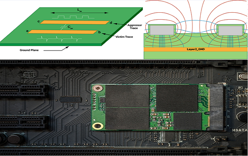
Crosstalk in High Speed PCB: Core Fundamentals
Definition & Electrical Mechanism
Crosstalk is the transfer of energy through capacitive and inductive coupling between aggressor and victim transmission lines.
- Capacitive coupling generates noise proportional to voltage slew rate (dV/dt).
- Inductive coupling generates noise proportional to current slew rate (dI/dt).
- Acceptable limit: Crosstalk noise ≤5% of signal amplitude (IPC-2221 generic standard).
- High-speed trigger: Signals with rise time ≤100ps or data rate ≥10Gbps exhibit severe coupling.
Impact on System Performance
- Voltage noise exceeding 5% triggers bit errors and eye closure in high speed pcb links.
- Differential pair skew increases by 20–40ps under strong crosstalk conditions.
- Radiated emissions rise by 10–15dBμV/m, violating CISPR 22 Class B limits.
- hdi pcb structures amplify crosstalk due to finer trace pitch and thinner dielectrics.
Learn more about: Controlled Impedance in High-Speed PCB: Full Tutorial
Causes of Crosstalk
Parallel Trace Routing
- Parallel routing beyond critical length saturates backward crosstalk at a fixed maximum value.
- Critical length formula: L_critical = (Tr × v) / 2, where v = velocity in PCB medium.
- Example: Tr=100ps, FR-4 velocity=6in/ns → L_critical=0.3in (7.6mm).
- Parallel runs exceeding critical length gain no additional crosstalk but maintain maximum noise.
Small Trace Spacing
- Crosstalk magnitude scales inversely with the square of trace separation distance.
- 4mil width traces require ≥12mil edge-to-edge spacing to meet −35dB crosstalk target.
- High frequency pcb designs need 5× width spacing for signals ≥25Gbps.
- Narrow spacing in hdi pcb (≤6mil) increases coupling by 300% compared to 12mil spacing.
High-Speed Signals & Fast Rise Time
- Noise amplitude directly scales with signal edge rate (dV/dt).
- 100ps rise time signals generate 5× more crosstalk than 500ps rise time signals.
- Maximum bandwidth formula: F_max = 0.5 / Tr.
- High speed pcb operation ≥5GHz requires strict physical separation rules.
Improper Layer Stack-up
- Adjacent parallel signal layers create vertical broadside coupling.
- Missing reference planes increase loop area and inductive coupling by 200%.
- Uneven dielectric thickness changes impedance and coupling coefficients.
- Asymmetric stackup causes warping and inconsistent spacing in mass production.
Common Types of Crosstalk
Near-End Crosstalk (NEXT)
- NEXT occurs at the driver end of the victim trace, also called backward crosstalk.
- Saturates at critical length and remains constant with longer parallel runs.
- Dominant noise source in high speed pcb and hdi pcb routing.
- Measurement reference: IPC-TM-650 2.5.5.12 for crosstalk qualification.
Far-End Crosstalk (FEXT)
- FEXT occurs at the receiver end of the victim trace, also called forward crosstalk.
- Increases linearly with coupled length but remains small in typical PCB dimensions.
- Negligible compared to NEXT for PCB-scale routing.
- Becomes significant only in backplanes or long flexible circuits.
Mitigation Techniques in PCB Design
Increase Trace Spacing
- Spacing is the most effective crosstalk control method.
- 3W rule: Spacing ≥3× trace width reduces crosstalk by ~80%.
- 5W rule: Spacing ≥5× width reduces crosstalk by ~95% for high speed pcb.
- Factory verified: 4mil traces need 12mil spacing for −35dB isolation.
Minimize Parallel Run Length
- Restrict parallel runs below critical length to avoid saturation.
- Stagger or break long parallel routes with orthogonal sections.
- Route high-risk nets with short parallel segments ≤200mil.
- hdi pcb BGA fanouts require intentional length breaking.
Solid Ground Planes
- Continuous reference planes provide low-impedance return paths and reduce loop area.
- Place signal layers directly adjacent to ground planes with ≤4mil dielectric.
- Eliminate plane gaps and slots under high-speed traces.
- Use stitching vias at 1mm pitch to bridge split planes.
Guard Traces
- Guard traces grounded with vias at ≤200mil pitch provide −15dB additional attenuation.
- Width ≥3mil and clearance ≥3mil to avoid capacitive loading.
- Effective in dense hdi pcb where spacing expansion is impractical.
- Factory caveat: Guard traces consume routing space and increase complexity.
Differential Pair Routing
- Differential signaling rejects common-mode noise by 20–30dB.
- Maintain tight, fixed spacing between paired traces.
- Length matching ≤5mil (≤25ps skew) preserves noise immunity.
- Preferred for PCIe, USB, Ethernet, and high frequency pcb links.
Learn more about: 10 Best Practices for High-Speed PCB Routing
Crosstalk Analysis Tools
Field Solver & SI Simulation
- 3D electromagnetic simulators calculate exact coupling coefficients.
- Predict NEXT/FEXT levels before physical prototyping.
- Validate stackup, spacing, and length rules across process corners.
- Essential for hdi pcb and high speed pcb sign-off.
Post-Production Testing
- TDR measurement for impedance and discontinuity analysis.
- Near-end and far-end crosstalk compliance testing.
- High-speed eye diagram verification.
- IPC-6012 Class 3 requires 100% electrical coupon testing.
Key Comparisons
| Crosstalk Control Method | Effectiveness | Routing Density Impact | Best For |
|---|---|---|---|
| 3W Spacing Rule | 80% reduction | Medium | Standard high speed pcb |
| 5W Spacing Rule | 95% reduction | High | High frequency pcb ≥25Gbps |
| Guard Traces | 40% reduction | Low | Dense hdi pcb |
| Differential Routing | 90% reduction | Medium | Differential interfaces |
| Crosstalk Type | Saturation Behavior | Dominant Range | Factory Priority |
|---|---|---|---|
| Near-End (NEXT) | Saturates at critical length | Full PCB length | Primary mitigation |
| Far-End (FEXT) | Linear increase | Long backplanes | Secondary concern |
Case Study: 12-Layer HDI High Frequency PCB
Project Specifications
- Layers: 12-layer symmetric stackup, high frequency pcb material (Dk=3.6).
- Data rate: 28Gbps NRZ, differential pairs at 100Ω impedance.
- Trace geometry: 4mil width, 5mil spacing, 4mil dielectric height.
- hdi pcb structure: Stacked microvias 0.12mm, sequential lamination.
Issues Encountered
- NEXT crosstalk level −22dB, well below −35dB requirement.
- Eye height collapsed to 0.22Vpp from 0.4Vpp target.
- Parallel routing over 1.2in (3x critical length) with 8mil spacing (2W rule).
- Broadside coupling between adjacent signal layers.
Improvements Implemented
- Expanded spacing from 8mil to 15mil (3.75W rule).
- Broke parallel runs into 200mil staggered segments.
- Inserted ground plane between signal layers to eliminate broadside coupling.
- Added guard traces with grounded vias in dense BGA areas.
Results
- Crosstalk improved to −36dB, fully compliant with IPC-2221.
- Eye height recovered to 0.39Vpp.
- Manufacturing yield increased from 78% to 96.5%.
- Radiated emissions reduced by 11dBμV/m.
| Case Study Aspect | Details / Parameters |
|---|---|
| Project Specifications | 12-layer symmetric stackup, high frequency pcb (Dk=3.6), 28Gbps NRZ, 100Ω differential pairs, 4mil width, 5mil spacing, hdi pcb 0.12mm microvias |
| Issues Encountered | Crosstalk −22dB (target −35dB), eye height 0.22Vpp, 1.2in parallel routes (3x critical length), 8mil spacing (2W), broadside coupling |
| Improvements Implemented | Spacing increased to 15mil (3.75W), parallel runs broken to 200mil staggered segments, ground plane inserted between signal layers, guard traces added |
| Results | Crosstalk −36dB (compliant), eye height 0.39Vpp, yield 78% → 96.5%, emissions reduced 11dBμV/m |
Common Design Errors
- Reliance on Guard Traces Instead of Spacing: Guard traces only reduce noise by ~40%, while spacing delivers ~95% improvement. Results in non-compliant boards.
- Parallel Routes Exceeding Critical Length: Creates maximum saturated NEXT regardless of additional length. Requires full rerouting.
- Adjacent Signal Layers Without Orthogonality: Vertical broadside coupling adds 20–30% extra noise. Cannot be fixed after etching.
- Plane Gaps Under High-Speed Traces: Destroys return path and increases crosstalk by 200%. Causes consistent production failures.
Quality Control & Compliance
Testing Protocols
- Coupon-level crosstalk measurement per IPC-TM-650.
- TDR impedance verification ±5% tolerance.
- Eye diagram testing at maximum operating data rate.
- 3D X-ray inspection of hdi pcb via structures and trace spacing.
Standards Compliance
- IPC-2221: Generic crosstalk and spacing requirements.
- IPC-6012: Qualification and performance of rigid PCBs.
- CISPR 22: Radiated emission limits from digital devices.
- PCIe/USB/Ethernet: Specific −35dB crosstalk mandate.
FAQ
Q1: What spacing rule is recommended for high speed pcb vs hdi pcb?
A1: High speed pcb uses the 3W rule (spacing ≥3× width). hdi pcb and high frequency pcb require the 5W rule (spacing ≥5× width) for −35dB crosstalk compliance at ≥10Gbps.
Q2: How does rise time influence crosstalk in high frequency pcb?
A2: Crosstalk increases linearly with faster rise times. A 100ps edge rate generates 5× more noise than 500ps. High frequency pcb operating ≥5GHz requires strict separation.
Q3: Are guard traces effective in hdi pcb design?
A3: Guard traces provide ~40% noise reduction but consume routing space. They are used only when spacing cannot be increased in dense BGA fanout regions of hdi pcb.
Q4: What is the difference between NEXT and FEXT in PCB design?
A4: NEXT (near-end) saturates at critical length and dominates PCBs. FEXT (far-end) increases linearly but remains negligible in typical board sizes. Factory mitigation focuses on NEXT.
Learn more about : What Is High-Speed PCB? A Comprehensive Guide


![Understanding PCB Costs & Pricing [Your Complete Guide]](https://hdicircuitboard.com/wp-content/uploads/elementor/thumbs/Understanding-PCB-Costs-Pricing-Your-Complete-Guide-qzzhe6mcaxuolkux3xalfktgavumi9y1aqfbs9bpv4.webp "Understanding PCB Costs & Pricing [Your Complete Guide]")


