
High speed differential pair routing is the backbone of reliable high-frequency interfaces, requiring strict adherence to length matching, impedance control, and symmetry to minimize crosstalk and preserve signal integrity. This guide details factory-proven rules, precise parameters, and interface-specific requirements tailored to hdi pcb, Low Loss PCB, and ultra low loss pcb applications.
Learn more about: What Is High-Speed PCB? A Comprehensive Guide
High Speed Differential Pair: Core Fundamentals
Definition & Critical Thresholds
- High speed differential pairs carry complementary signals (equal magnitude, opposite polarity) with data rates ≥1Gbps or edge rates ≥1V/ns, per IPC-2221.
- Key advantage: Common-mode noise rejection, critical for reducing EMI in dense hdi pcb layouts.
- Performance benchmark: Differential impedance tolerance ±5% (IPC-6012 Class 3) to avoid reflections.
Material Impact on Performance
- Low Loss PCB (Df=0.004–0.009 @10GHz) supports 5–25Gbps, ideal for mid-speed interfaces like USB 3.0.
- ultra low loss pcb (e.g., Rogers RO4350B, Df=0.0037 @10GHz) enables ≥25Gbps (PCIe 5.0/Ethernet 400G) with 40% lower insertion loss.
- hdi pcb requires materials with low CTE (X/Y ≤16ppm/°C) to maintain pair spacing during sequential lamination.
Learn more about: Signal Integrity in HDI PCB Design
Differential Pair Routing Rules: Foundational Principles
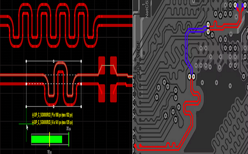
Length Matching
- Tolerance standards: ≤5mil (≤25ps skew) for ≥10Gbps signals; ≤3mil (≤15ps) for ≥25Gbps.
- Tuning method: Serpentine traces with pitch ≥5x trace width (e.g., 20mil pitch for 4mil width) to avoid impedance discontinuities.
- Segment matching: Compensate length differences in each trace segment (e.g., via transitions, bends) individually, not just total length.
Constant Impedance & Symmetry
- Target values: 90Ω (USB 3.0/3.1), 100Ω (HDMI 2.0/PCIe/Ethernet) ±5% tolerance, per interface specs.
- Symmetry requirements: Identical trace width (4mil for 100Ω differential on 0.4mm FR-4) and spacing across the entire path.
- Manufacturing control: Impedance coupons (100mm length) included on every panel for TDR validation.
Pair Spacing
- Intra-pair spacing: 4–6mil for 4mil trace width (maintains differential impedance); no variation >1mil along the path.
- Inter-pair isolation: ≥3x intra-pair spacing (e.g., 12mil between 100Ω differential pairs) to reduce crosstalk ≤-35dB.
- hdi pcb adjustment: Reduce intra-pair spacing to 3mil in dense regions (0.5mm BGA pitch) but revert to 4mil post-breakout.
Avoiding Vias and Bends: Minimizing Discontinuities
Via Usage Guidelines
- Microvias (0.1–0.15mm diameter) for hdi pcb: Aspect ratio ≤1:1 (IPC-6016) to reduce inductance (≤1.2nH per via).
- Symmetric placement: Equal number of vias (max 2 per pair) for both traces, placed within 50mil of each other.
- Back-drilling: Remove via stubs to ≤3mil for signals ≥25Gbps (reduces reflection loss by 40%).
Bend Design Standards
- Avoid 90-degree bends: Use 45-degree angles or curved traces (radius ≥3x trace width) to prevent impedance spikes.
- Inner bend compensation: Add 2mil length to inner traces at bends to maintain symmetry.
- Differential pair bends: Keep both traces in the pair bent identically—no single-trace bends.
Reference Planes & Layer Selection
Reference Plane Requirements
- Solid ground plane: Continuous with ≤50mil gaps; stitching vias (1mm pitch) to connect split planes.
- Adjacent planes: Signal layers paired with ground planes in hdi pcb (1+N+1 stackup) to reduce loop inductance.
- No routing over splits: If unavoidable, place 10nF–100nF stitching capacitors within 20mil of the signal path.
Layer Selection Criteria
- Preferred layers: Outer layers (microstrip) for ≤25Gbps; inner layers (stripline) for ≥25Gbps (reduces crosstalk by 30%).
- Layer transitions: Minimize cross-layer routing; if required, use identical via configurations for both traces.
- ultra low loss pcb: Route critical pairs (PCIe 5.0) on inner layers with dielectric thickness ≤0.1mm for stable impedance.
Common High-Speed Interfaces: Interface-Specific Rules
USB 3.0/3.1
- Differential impedance: 90Ω ±5% (IPC-2221), with trace width 4mil and spacing 5mil.
- Length matching: Skew ≤400ps (equivalent to 60mm trace difference).
- Placement: AC coupling capacitors (0402 package) symmetrically within 50mil of the connector; no test points on signal paths.
HDMI 2.0
- Differential impedance: 100Ω ±5% for TMDS pairs, with trace width 4mil and spacing 6mil.
- Length matching: ±3mm between TMDS pairs; skew ≤100ps.
- hdi pcb requirement: Ground vias within 20mil of HDMI connector pins to reduce EMI.
PCIe/Ethernet
- PCIe (Gen 5): 100Ω ±5% differential impedance, length matching ≤3mil (≤15ps skew); max 2 vias per pair.
- Ethernet (400G): ultra low loss pcb mandatory (Df ≤0.004), differential impedance 100Ω ±5%, pair spacing 5mil.
- Common rule: Keep parallel runs between pairs ≤500mil to limit crosstalk.
Learn more about: 50Ω / 75Ω / 100Ω Impedance in High Density Interconnect (HDI) PCBs: Design & Production Guide
Key Comparisons
| Routing Parameter | Low Loss PCB (5–25Gbps) | Ultra Low Loss PCB (≥25Gbps) |
|---|---|---|
| Differential Impedance | 90–100Ω ±5% | 90–100Ω ±3% |
| Length Matching Tolerance | ≤5mil | ≤3mil |
| Pair Spacing | 4–6mil | 5–7mil (tighter coupling) |
| Insertion Loss Target | ≤0.3dB/inch @20GHz | ≤0.2dB/inch @20GHz |
| Interface | Differential Impedance | Skew Tolerance | Preferred Material |
|---|---|---|---|
| USB 3.0/3.1 | 90Ω ±5% | ≤400ps | Low Loss PCB (FR408HR) |
| HDMI 2.0 | 100Ω ±5% | ≤100ps | Low Loss PCB (Isola I-Speed) |
| PCIe 5.0 | 100Ω ±3% | ≤15ps | ultra low loss pcb (Rogers RO4350B) |
| Ethernet 400G | 100Ω ±3% | ≤10ps | ultra low loss pcb (Megtron 7) |
Quality Control & Validation
Testing Protocols
- TDR impedance testing: Verify differential impedance within ±5% (±3% for ultra low loss pcb).
- Crosstalk measurement: ≤-35dB for adjacent pairs (IPC-TM-650 2.5.5.12).
- Eye diagram analysis: Eye height ≥0.3Vpp, jitter ≤10% of bit period for ≥25Gbps.
Manufacturing Checks
- Trace width/spacing: ±0.5mil tolerance (IPC-2221) to maintain impedance.
- Via inspection: X-ray verification of microvia fill (≥95% for hdi pcb).
- Thermal cycling: 1000 cycles (-40°C~125°C) to confirm pair stability (no spacing drift).
Case Study: 12-Layer HDI Ultra Low Loss PCB
Project Specifications
- Layers: 12 (4+4+4 stackup), interface: PCIe 5.0 (32Gbps), material: Rogers RO4350B (Df=0.0037 @10GHz).
- Routing parameters: 100Ω differential impedance, trace width 4mil, spacing 5mil, skew ≤15ps.
- hdi pcb features: Stacked microvias (0.12mm diameter), sequential lamination (3 cycles).
Issues Encountered
- Crosstalk (+18dB) between adjacent PCIe pairs (spacing=3mil, below 3x intra-pair spacing).
- Skew (22ps) exceeding tolerance due to asymmetric via placement.
- Impedance deviation (+7%) from uneven dielectric thickness in inner layers.
Improvements Implemented
- Increased inter-pair spacing to 15mil (-34dB crosstalk).
- Symmetric via placement (2 vias per pair) and serpentine tuning (3mil length addition) to reduce skew to 12ps.
- Adjusted trace width to 4.2mil and verified dielectric thickness (0.1mm ±0.005mm) to correct impedance.
Results
- Signal integrity compliance: Eye height=0.4Vpp, jitter=28ps.
- Manufacturing yield: 97.3% (up from 81% initial run).
- EMI emissions: 27dBμV/m (meets CISPR 22 Class B).
| Case Study Aspect | Details / Parameters |
|---|---|
| Project Specifications |
• Layers: 12 (4+4+4 stackup) • Interface: PCIe 5.0 (32Gbps) • Material: Rogers RO4350B (Df=0.0037 @10GHz) • Routing parameters: 100Ω differential impedance, 4mil width, 5mil spacing, skew ≤15ps • HDI PCB: Stacked microvias (0.12mm diameter), sequential lamination (3 cycles) |
| Issues Encountered |
• Crosstalk (+18dB): Adjacent PCIe pairs (spacing=3mil, below 3x intra-pair spacing) • Skew (22ps): Exceeded 15ps tolerance (asymmetric via placement) • Impedance deviation (+7%): Uneven dielectric thickness in inner layers |
| Improvements Implemented |
• Increased inter-pair spacing to 15mil (crosstalk reduced to -34dB) • Symmetric via placement + 3mil serpentine tuning (skew to 12ps) • Adjusted trace width to 4.2mil, verified dielectric thickness (0.1mm ±0.005mm) |
| Results |
• Signal integrity: Eye height=0.4Vpp, jitter=28ps (compliant with PCIe 5.0 specs) • Manufacturing yield: 97.3% (up from 81%) • EMI emissions: 27dBμV/m (CISPR 22 Class B compliant) |
Common Design Errors
- Asymmetric Pair Routing: Uneven trace widths (±1mil) cause impedance mismatch (+10%)—requires redesign of trace geometry (cost +$0.70/board).
- Overlooking Via Stubs: Unback-drilled vias (10mil stub) for 25Gbps signals increase reflection loss by 25%—back-drilling adds $0.30/via.
- Inadequate Ground Planes: Split ground planes under differential pairs increase crosstalk by 15x—requires copper filling and stitching capacitors.
- Material Mismatch: Using Low Loss PCB for PCIe 5.0 (≥32Gbps) leads to 30% higher insertion loss—full board redesign with ultra low loss pcb.
FAQ
Q1: What’s the difference between Low Loss PCB and ultra low loss pcb for differential pair routing?
A1: Low Loss PCB (Df=0.004–0.009 @10GHz) works for 5–25Gbps (USB 3.0/HDMI 2.0), while ultra low loss pcb (Df≤0.004) supports ≥25Gbps (PCIe 5.0/Ethernet 400G) with superior noise rejection and impedance stability.
Q2: How to handle length matching in dense hdi pcb layouts?
A2: Use minimal serpentine tuning (close to mismatched segments) with pitch ≥5x trace width. For 0.5mm BGA pitch, reduce intra-pair spacing to 3mil temporarily but maintain symmetry and revert to 4mil post-breakout.
Q3: What via type is best for high speed differential pair routing in hdi pcb?
A3: Stacked microvias (0.1–0.15mm diameter) with back-drilling (stub ≤3mil) are optimal. They reduce inductance by 70% vs. through-hole vias and support dense fanout for fine-pitch BGAs.
Q4: How to validate differential pair routing before manufacturing?
A4: Run SI simulation (HyperLynx/SIwave) to check crosstalk, skew, and impedance. Request impedance coupons from fabricators and perform TDR testing. Produce a test coupon with 3–5 pair samples to verify manufacturing consistency.
If you need high speed PCB manufacturing or design support,our engineering team provides free DFM analysis and quotation.


![Understanding PCB Costs & Pricing [Your Complete Guide]](https://hdicircuitboard.com/wp-content/uploads/elementor/thumbs/Understanding-PCB-Costs-Pricing-Your-Complete-Guide-qzzhe6mcaxuolkux3xalfktgavumi9y1aqfbs9bpv4.webp "Understanding PCB Costs & Pricing [Your Complete Guide]")


