
There’s a lot that goes into the design and fabrication of a printed circuit board, but the assembly process is just as important. If you aren’t using a reputable provider who follows best practices, your project could end up facing costly delays.
Keep reading to learn more about the entire PCB assembly process — including a step-by-step guide.
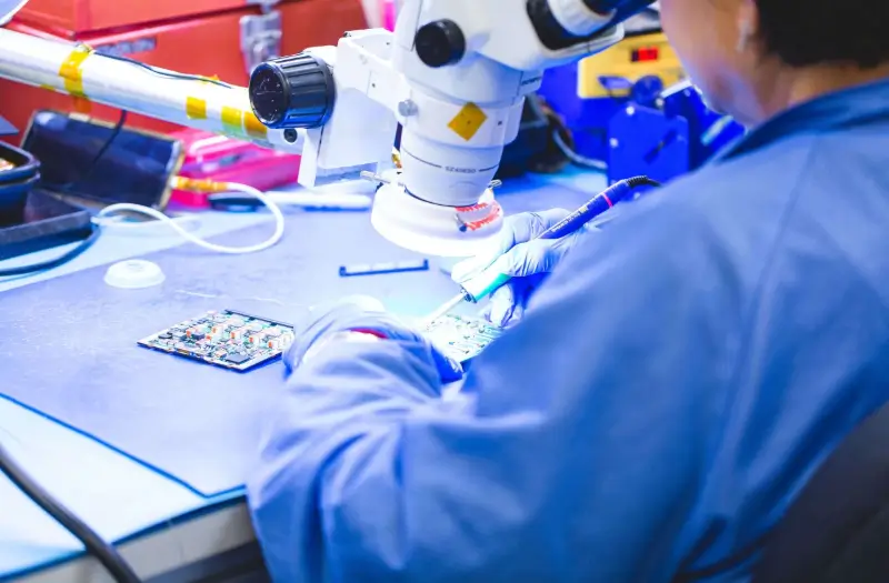
PCB Assembly Basics: Designing a Board for Success
Printed circuit board assembly (also known as PCBA) is the process of mounting a fabricated board with the correct components. But you can’t assemble a board if it isn’t designed correctly.
First, let’s explore the typical makeup of a printed circuit board, including materials and components.
- Substrate — This refers to the supporting material that holds the components and traces.
- Copper — This element is used in printed circuit boards due to its highly conductive electrical components.
- Solder mask — This is a technique in which all parts of a circuit board are coated with epoxy, except the contacts that need to be soldered, the gold-plated terminals of any card-edge connectors, and fiducial marks.
- Silkscreen — Though this doesn’t impact a PCB’s function, it’s worth mentioning. A silkscreen refers to digitally printed legend that outlines the decals and references designators in epoxy ink printed on the board. A silkscreen will help you recognize warning symbols and identify components and where they should be placed.
- Annular ring — This refers to the copper ring surrounding the holes on a board.
- Trace and space — A trace is the copper structure that the signals travel through — commonly referred to as a wire.
- Thru-hole or surface mount components — Components refer to any basic part that is used in building electrical equipment, such as resistors, capacitors, fuses, etc.


![Understanding PCB Costs & Pricing [Your Complete Guide]](https://hdicircuitboard.com/wp-content/uploads/elementor/thumbs/Understanding-PCB-Costs-Pricing-Your-Complete-Guide-qzzhe6mcaxuolkux3xalfktgavumi9y1aqfbs9bpv4.webp "Understanding PCB Costs & Pricing [Your Complete Guide]")
![Determining PCB Via Size [w Guidelines]](https://hdicircuitboard.com/wp-content/uploads/elementor/thumbs/Determining-PCB-Via-Size-w-Guidelines-qzzhe6mcaxuolkux3xalfktgavumi9y1aqfbs9bpv4.webp "Determining PCB Via Size [w Guidelines]")
![PCB Material Types Explained [Your Guide]](https://hdicircuitboard.com/wp-content/uploads/elementor/thumbs/PCB-Material-Types-Explained-Your-Guide-qzzhe6mcaxuolkux3xalfktgavumi9y1aqfbs9bpv4.webp "PCB Material Types Explained [Your Guide]")

