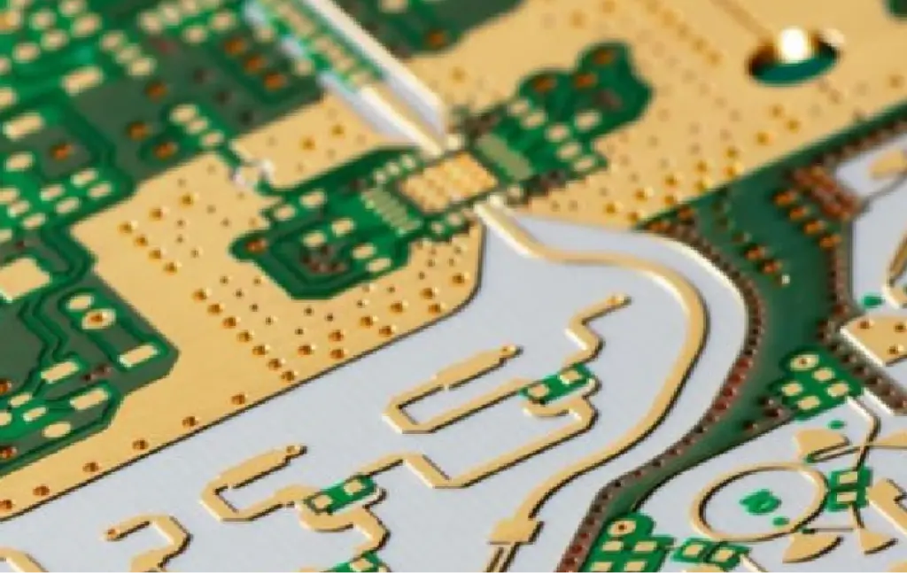
Blind and/or buried via, built-up laminations
High frequency low loss PCB material, low loss high speed PCB materials, Rigid-flex and flexible PCB manufacturer
HDI blind and buried microvias,built-up laminations
High frequency low loss PCB material, low loss high speed PCB materials, Rigid-flex and flexible PCB manufacturer
HDI blind and buried microvias,built-up laminations
High frequency low loss PCB material, low loss high speed PCB materials, Rigid-flex and flexible PCB manufacturer
HDI blind and buried microvias, built-up laminations
High frequency low loss PCB material, low loss high speed PCB materials, Rigid-flex and flexible PCB manufacturer
Blind and/or buried via, Fine line and fine pitch BGA
High frequency low loss PCB material, low loss high speed PCB materials, Rigid-flex and flexible PCB manufacturer
HDI Blind and Buried Microvias, Fine line and fine BGA pitch
High frequency low loss PCB material, low loss high speed PCB materials, Rigid-flex and flexible PCB manufacturer
High Density Interconnect
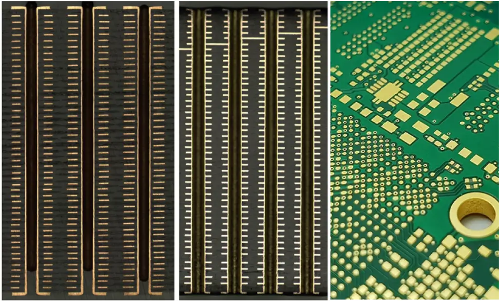
PCB Manufacturing
As a leading manufacturer of advanced interconnect solutions for medical devices, Telecom, Industrial, Automotive and Computing. Benchuang Electronics specializes in flexible, rigid-flex, rigid technologies and pcb assembly, providing highly complex HDI or ultra HDI PCB, high frequency and high reliability printed circuit boards for medical, high frequency and semiconductor applications.
Our flexible printed circuits offer reliable performance and durability, meeting the demanding requirements of IPC Class 3 standards with a focus on technical excellence.
- High frequency PTFE, Ceramic, Polyimide based material in stock; RO3000 and RO 4000 series RT6012, RT5870/5880, TMM10i, Arlon 85N,32N, tachyon 100G..etc,
- Panasonic Megtron 6,7 and 8 for those Networking equipment s require an extremely low transmission loss for high Speed communication
- High density PCB boards with high pin counts with fine BGA pitch down to 0.15 mm. The closest distance between the rims of vias to circuitries is by 2.50 mils
- Down to 0.03mm trace space, 0.05 mm holes
- Blind vias, buried vias, and other microvia techniques
- Built-up laminations and high-signal performance considerations
- Laser drill and Laser direct Imaging
- Fine lines and via-in-pad technology
- Single Sided Flexible PCB,Double Sided Flex PCB, Multilayer Flex PCB, Transparent Flexible PCB, Sculptured Flex Circuits, HDI Flex PCB
- Rigid Flex PCB
- One-stop for PCB prototype and Assembly
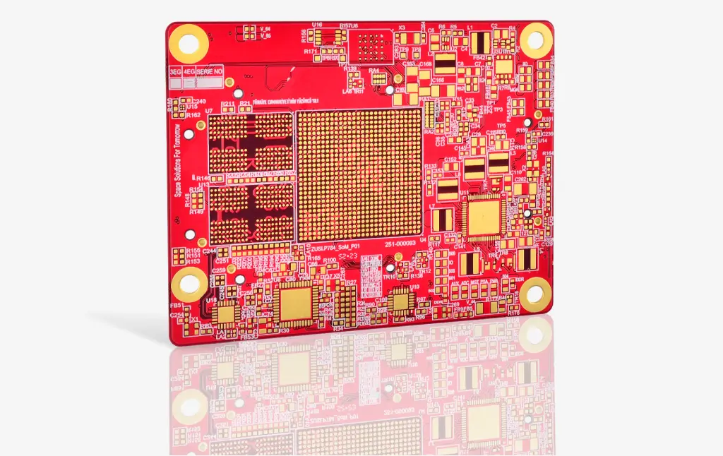
HDI PCB
HDI PCBs are characterized by thin lines, closer spaces, and more dense wiring, which allow for a faster connection while reducing the size and bulk of a project. These boards also feature blind and buried vias, laser-drilled microvias, sequential lamination, and via in-pads.
We use the most advanced equipment and technology, including laser direct imaging, to hold tight tolerances so that we can meet today’s HDI PCB requirements.
HDI Circuit Board Features
- Layer count: 4~40L
- Board material: Ro4350B、Ro4003C、M6 series 、M7 series、EMC528(HF)、EMC891~K、EMC890~890K(HF)、Isola I-Tera、Isola TerraGreen、Tuc-933、Tuc-883
- Board thickness: 0.18mm min.
- Size: 18″ X 23″ (Shipping size)
- BGA Pitch: 0.35mm (min)
- Min trace width/spacing: 0.003″/0.003″
- Min thru hole size: 6mils (VIP resin filled) 8mils (VIP copper paste plugged)
- Min gap from PTH to track inner layers: > 6mils
- Thru hole aspect ratio(The board thickness vs. Drill hole size): 8~30
- Min/Max Laser drill hole size: 3mils / 8mils ( VIP plated shut)
- Aspect ratio (dielectric thickness/ Laser drill hole size): 0.8Max.
- HDI: 10+N+10(Anylayer)
- Back drill: Min hole size 15.7mils Depth tolerance +/-6mils
- Copper coin: length x width 3mm x 3mm(min) Surface flatness:30um(max)
- Layer to Layer Registration: +/-1.5mils min.
- Tolerance of impedance control: +/-5%
- Cavity Process: Laser cutting
- Board finishings: ENEPIG+Hard gold plating(Gold finger) Soft gold plating+Hard gold plating(Gold finger)
Ultra HDI PCB Features
- Lines/spaces: 25/35 μm
- Microvias/pads Ø: 50/150 μm
- Thinnest starting material: 75 μm
- Thinnest dielectric thickness: 50 μm
- Conductor width tolerance: +/- 10%
- Artwork to soldermask tolerance: +/- 15 μm
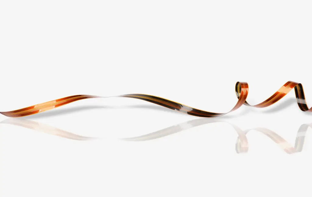
Flexible PCB
Flexible printed circuit boards (FPC) are offering the highest level of 3D miniaturization. Very low bending radii in combination with ultra-HDI (ultra-high density interconnect) are enabling our customers to build increasingly smaller and highly integrated devices. This technology is an enabler of small wearable devices as well it provides high signal density.
Benchuang Electronics has been a market leader in this field for many years and is manufacturing flex circuits with a layer-count of 1 to 16. We are working with polyimide foils as thin as 12.5 µm (0.5 mil) and adhesive bond plys starting at a thickness of 12.5 µm (0.5 mil). Our state of the art equipment is enabling us to produce FPCs with high output, reliability and repeatability. Depending on the dielectric thickness, laser drilled blind vias can be as small as 30 µm (1.4 mil) in diameter, and can be filled with copper in the subsequent plating process. This plating technology is enabling the use of stacked vias and via-in-pad structures.
Technological Highlights
- Turnkey flex solutions targeting 3D miniaturization
- Highly reliable, extremely robust multilayer flex/microvia substrates
- Ultra-thin base materials
- Filled via and stacked via process available
- Complex mechanical/assembly assist features, including special profiles, fold lines, cut-outs and thinned bending zones/cavities
- Wrap-around boards
- Chip-on-flex (COF), chip scale packaging (CSP) substrates, and BGAs
- A wide variety of surface finishes, for example; OSP, ENIG, ENEPIG, E-AU, DIG
- Flying leads
- Bending test for flexible circuits
- Ultra-fine line flex cables
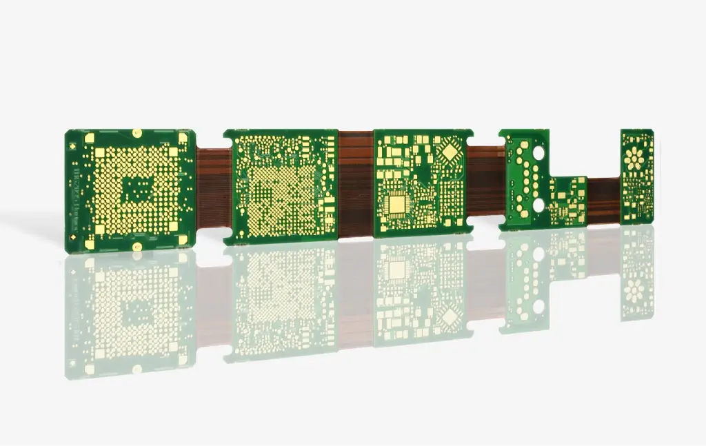
Rigid Flex PCB
A technology that combines the best of two worlds – the stability of rigid boards and the flexibility of flexible circuits, pun intended!
Rigid flex circuit boards offer the best in packaging technology by merging the flexibility of flex circuits with the dense packaging of traditional rigid circuit boards. Combining the component and routing density of hardboards with the flexibility of flexible circuits, rigid flex PCBs allow designers to achieve routing density and interconnectivity that is not available in other types of circuit boards.
Benchuang Electronics is offering a big variety of rigid-flex PCB constructions, using high end/quality base materials, like high TG/low CTE FR4, combined with polyimide foils and various adhesives. State of the art interconnection technologies like stacked or staggered vias and via-in-pad structures are used to drive miniaturization further down the road. A big portfolio of surface finishings is enabling Benchuang Electronics' customers to use all available assembly methods on boards produced by us.
Rigid Flex PCB Features
- Available in layer counts above 20 layers for very high routing density
- Flexible layers typically 1, 2, 3 or 4, though more can be accommodated
- Controlled impedance in both rigid & flexible sections
- Very high reliability
- Minimum dielectrics: down to 1 mil in flex sections, 2 mil in rigid sections
- Largest library of rigid flex constructions approved to UL 94 V-0
- RoHS compliant
RF PCB
Benchuang Electronics has been providing trusted PCB manufacturing and fabrication services since 2007. We pride ourselves on having the deep engineering experience and advanced technology and equipment to handle any project all the way from layout through assembly in our state-of-the-art facility. This includes fabrication and manufacturing of radio frequency (RF) and microwave PCBs.
RF PCB Capabilities
- Layer count: 2~20L
- Board material: RO4350 B、Isola Astra MT77、RF35、RO4003 C、Ro3003、Ro3010、RT5870、RT5880、RT6010、Ro4360、TMM10、TMM10i、TACONIC RF series、TACONIC TLY series
- Double-sided process: RT5870、RT5880、RT6010、Ro4360、TMM10、TMM10i
- Hybrid: Ro3003、Ro3010、Ro4360、TACONIC RF series、TACONIC TLY series+ FR4
- Board thickness: 0.18mm(min)
- Size: 0.5″ X 0.5″ (min)(Shipping size)
- Min trace width/spacing: 0.005″/0.005″
- Tolerance of trace width / spacing: +/-8% trace width > 10mils and tolerance: +/-1mils
- Radius of Antenna width: 0.5mils(max)
- Min gap from Antenna to conductors: 3mils(min)
- Min thru hole size: 6mils (VIP resin filled) 8mils (VIP copper paste plugged)
- Min gap from hole edge to hole edge (Stitching via): 8mils
- Min gap from hole edge to copper (Stitching via): 6mils
- Aspect ratio: dielectric thickness / Laser drill hole size: 5mils / 6.50 mils(max) ( VIP plated shut )
- HDI: 6+N+6
- Layer to Layer Registration: +/-1.50 mils
- Tolerance of impedance control: +/-5%
- Cavity Process: Lamination (Adhesive Low Dk Low Df)+depth control milling
- Conductive via fill, Non-conductive via fill, Plated edges, Plated radii (castellation), Plated milling cutouts, Hard gold body, Soft bondable gold, Immersion gold, Immersion silver, HAL standard, HAL lead-free (ROHS), ENTEK (OSP)
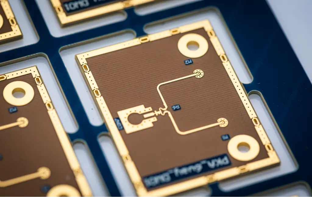
High Frequency PCB
When it comes to high frequency PCB design, it’s important that the design engineer collaborate with the PCB supplier to select the materials for the desired frequency performance requirements and to establish the correct stack-up. Benchuang has deep engineering capabilities and experience with control depth drilling, control depth milling, and back drilling, unlike some of our competitors. This means we have the technology, the experience, and the knowledge to help you design and build the right high frequency PCB from the start.
We differentiate ourselves by being able to take on all complex jobs — all the way from layout through assembly — and we do this under one roof with state-of-the-art technology and an extensive engineering team. This end-to-end expertise allows us to excel at the entire process and be the best PCB provider in the word.
High Frequency PCB Capabilities
- Hybrid or Mixed Dielectric Boards (PTFE/FR-4 combinations)
- Board material: I-Speed、I-Tera® MT40、Tachyon-100G、Isola Astra MT77、Megtron 6 R-5775、Megtron 7 R-5785、Megtron 7N R-5785N、RO4350 B、RO4835、RO4003、RO4533、IT-968、IT-968 SE、IT-988G、IT-988G SE、EM-528K、EM-890K、TU-883、TU-883SP
- Cavity Boards (Mechanical and Laser Drilled)
- Edge Plating
- Constellations
- Large Format PCBs
- Front to back registration of etched cores to +/-0.05 mm
- +/- 0.0.025 mm tolerance on etched features for un-plated 1oz copper
- Blind/Buried, Via-in-Pad, Micro Vias, Stacked Vias, and Laser Via’s
- Soft Gold and ENEPIG Plating
- Sequential lamination
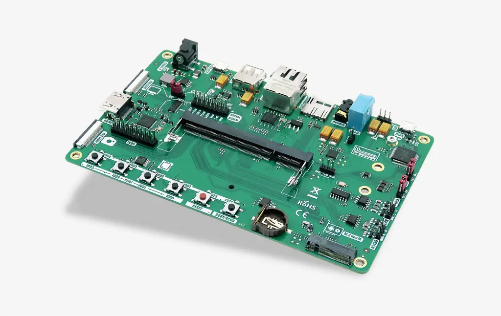
PCB Assembly
Benchuang Electronics is a reliable full turnkey PCB service solution for prototype quantities as well as small-volume to large-volume production runs, and a one stop PCB manufacturing and assembly company. As a provider of turnkey PCB services, our company offers professional consulting in Design for Manufacturing (DFM). Benchuang Electronics provides its customers with access to full turn-key, partial, and consigned assembly services, which means you have the option to buy the parts yourself (consigned) or allow us to take care of that for you (turn-key).Our integrated fabrication and assembly services ensure a smooth transition since everything is completed within the same building. By shortening the supply chain, you eliminate outside factors that can lead to delays and errors.
PCB Assembly capabilities
- SMT, Through Hole and Mixed Assembly
- Passive Down to 01005 Sizes
- Ball Grid Array (BGA)
- Ultra-Fine Ball Grid Array (uBGA)
- Quad Flat Pack No-Lead (QFN)
- Quad Flat Package (QFP)
- Plastic Leaded Chip Carrier (PLCC)
- SOIC, Package-On-Package (PoP)
- Small Chip Packages (Pitch of 0.2 mm)
- BGA, micro-BGA, QFN, CSP and any leadless devices up to .20mm pitch assembly with 100% 3D X-ray inspection
![Determining PCB Via Size [w Guidelines]](https://hdicircuitboard.com/wp-content/uploads/elementor/thumbs/Determining-PCB-Via-Size-w-Guidelines-qzzhe6mcaxuolkux3xalfktgavumi9y1aqfbs9bpv4.webp "Determining PCB Via Size [w Guidelines]")
![PCB Material Types Explained [Your Guide]](https://hdicircuitboard.com/wp-content/uploads/elementor/thumbs/PCB-Material-Types-Explained-Your-Guide-qzzhe6mcaxuolkux3xalfktgavumi9y1aqfbs9bpv4.webp "PCB Material Types Explained [Your Guide]")


Get Touch For PCB Fabrication and Assembly
We’re here for you, and we look forward to serving you.