- Blind vias, buried vias, Ultra HDI PCB
- High frequency low loss PCB material
- TLY-5, RF35, RF-35TC, TSM-DS3, TLX-8, TLX-9 material
- RO4003, RO4350B, RO4835, RT/duroid 5870, RT/duroid 5880, RT/duroid 6002, TMM3, TMM4, TMM6, TMM10, TMM10i material
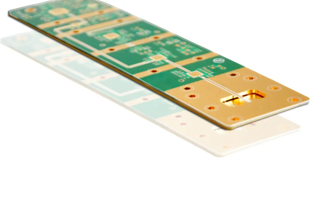
High Frequency PCB
Any PCB that operates at a frequency of 100MHz or above can be considered a high-frequency PCB. The laminate materials used to manufacture such boards feature low dielectric constant, high CTE, low loss tangent, and advanced composites. These boards are used in military, medical, and advanced communication applications such as GPS, radar, and base stations.
A high frequency printed circuit board, whether it’s rigid or flex, offers faster signal flow rates and a frequency range of up to 100 GHz. It’s important to note that there are numerous materials designed to operate at high frequency levels. HF PCBs are defined by lower dielectric constant (Dk), lower dissipation factor (Df), and low levels of thermal expansion. They are used regularly for HDI PCB technology. They are also used extensively in high speed communications, telecommunications, and RF microwave technology.
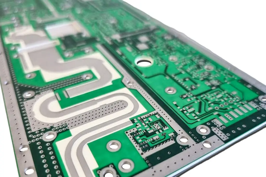
High Frequency PCB Capabilities
When it comes to high frequency PCB design, it’s important that the design engineer collaborate with the PCB supplier to select the materials for the desired frequency performance requirements and to establish the correct stack-up. Benchuang Electronics has deep engineering capabilities and experience with control depth drilling, control depth milling, and back drilling, unlike some of our competitors. This means we have the technology, the experience, and the knowledge to help you design and build the right high frequency PCB from the start.
High frequency PCB Design Guidelines
Download our design guidelines for high frequency PCBs
To prevent getting it wrong from the start, we have put together our design guidelines, to use as a checklist.
The file lists some of the fabrication features that are typically associated with high frequency PCB. The feature limits listed are not comprehensive; Our experienced engineers have also worked with every type of PCB material, so they have the knowledge and expertise to provide recommendations and answer all of your high frequency PCB questions. Most importantly, they know how to assist for manufacturability and the potential cost drivers of a project.
| Description | Production | Advanced |
|---|---|---|
| Inner Layer | ||
| Min.Trace/Space | 1.5mils / 1.5mils | 1.2mils / 1.5mils |
| Min. Copper Thickness | 1/3oz | 1/7 oz |
| Max. Copper Thickness | 10oz | 30oz |
| Min. Core Thickness | 2mils | 1.5mils |
| Line/ pad to drill hole | 7mils | 6mils |
| Line/ pad to board edge | 8mils | 7mils |
| Line Tolerance | +/-10% | +/-10% |
| Board Dimensions | ||
| Max. Finish Board Size | 19”X26” | 20”X28” |
| min. Finish Board Size | 0.2"X0.2" | 0.15"X0.15" |
| Max. Board Thickness | 0.300"(+/-10%) | 0.350"(+/-8%) |
| Min. Board Thickness | 0.007"(+/-10%) | 0.005"(+/-10%) |
| Lamination | ||
| Layer Count | 60L | 100L |
| Layer to Layer Registration | +/-4mils | +/-2mils |
| Drilling | ||
| Min. Drill Size | 6mils | 5mils |
| Min. Hole to Hole Pitch | 16mils(0.4mm) | 14mils(0.35mm) |
| True position Tolerance | +/-3mils | +/-2mils |
| Slot Diameter Tolerance | +/-3mils | +/-2mils |
| Min gap from PTH to track inner layers | 7mils | 6mils |
| Min. PTH edge to PTH edge space | 9mils | 8mils |
| Plating | ||
| Max. Aspect Ratio | 28:1 | 30:1 |
| Cu Thickness in Through hole | 0.8-1.5 mils | 2 oz |
| Plated hole size tolerance | +/-2mils | +/-1.5mils |
| NPTH hole tolerance | +/-2mils | +/-1mils |
| Min. Via in pad Fill hole size | 6mils | 4mils |
| Via in pad Fill Material | Epoxy resin/Copper paste | Epoxy resin/Copper paste |
| Outer Layer | ||
| Min. Trace/Space | 2mils / 2mils | 1.5mils / 1.5mils |
| Min. pad over drill size | 6mils | 5mils |
| Max. Copper thickness | 12 oz | 30 oz |
| Line/ pad to board edge | 8mils | 7mils |
| Line Tolerance | +/-15% | +/-10% |
| Metal Finish | ||
| HASL | 50-1000u” | 50-1000u” |
| HASL+Selective Hard gold | Yes | Yes |
| OSP | 8-20u” | 8-20u” |
| Selective ENIG+OSP | Yes | Yes |
| ENIG(Nickel/Gold) | 80-200u”/2-9 u” | 250u”/ 10u” |
| Immersion Silver | 6-18u” | 6-18u” |
| Hard Gold for Tab | 10-80u” | 10-80u” |
| Immersion Tin | 30u”min. | 30u” min. |
| ENEPIG (Ni/Pd/Au) | 125u"/4u"/1u” min. | 150u"/8u"/2u” min. |
| Soft Gold (Nickel/ Gold) | 200u”/ 20u”min. | 200u”/ 20u” |
| Solder Mask | ||
| S/M Thickness | 0.4mils min. | 2mils max. |
| Solder dam width | 4mils | 3mils |
| S/M registration tolerance | +/-2mils | +/-1.5mils |
| S/M over line | 3.5mils | 2mils / 2mils |
| Legend | ||
| Min. Space to SMD pad | 6mils | 5mils |
| Min. Stroke Width | 6mils | 5mils |
| Min. Space to Copper pad | 6mils | 5mils |
| Standard Color | White , Yellow, Black | N/A |
| Electrical Testing | ||
| Max. Test Points | 30000 Points | 30000 Points |
| Smallest SMT Pitch | 16mils(0.4mm) | 12mils(0.3mm) |
| Smallest BGA Pitch | 10mils(0.25mm) | 6mils(0.15mm) |
| NC Rout | ||
| Min. Rout to copper space | 8mils | 7mils |
| Rout tolerance | +/-4mils | +/-3mils |
| Scoring (V-cut) | ||
| Conductor to center line | 15mils | 15mils |
| X&Y Position Tolerance | +/-4mils | +/-3mils |
| Score Anger | 30o/45o | 30o/45o |
| Score Web | 10mils min. | 8mils min. |
| Beveling | ||
| bevel anger | 20-71o | 20-71o |
| Bevel Dimensional Tolerance | +/-10mils | +/-10mils |
| Impedance controll | ||
| Impedance controll | +/-10% | +/-7% |
View More +
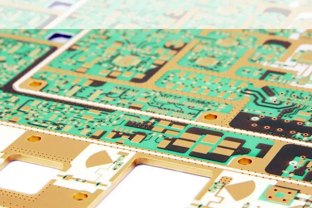
High Frequency PCB Materials
Special materials are required to achieve the high frequency provided by this type of PCB. There are a variety of substrate materials that will support your design and may differ based on signal speeds required and the application/environment of the circuit board.
In terms of price, FR4 is the least expensive compared to dedicated high speed materials and Teflon, with Teflon being the most expensive. Though, FR-4 starts to drop off in performance when signal speed edges above 1.6ghz
Newer generation substrates, Teflon, and flex circuits are the best options when it comes to Dk, Df, water absorption, and survivability in the environment
If a printed circuit board requires a frequency above 10GHz, newer generation substrates, Teflon, and Flex substrates are your best option since they are far superior to traditional FR-4 material.
The most common suppliers of high speed substrates are Rogers, Isola, Taconic and Megtron materials by Panasonic. All of these materials typically are lower Dk and lower loss.
High Frequency PCB Material Properties
There are a few material properties that should receive focus when shopping for high frequency PCB materials. There are multiple vendors that produce these materials, and they all try to compete with each other based on the electromagnetic properties for the materials they produce. You can spot all of the material properties I’ll specify below in the datasheest provided by the vendor.
Dk and Df (Loss Tangent)
This is probably the most common point everyone will start looking for when they dive into datasheets. Material vendors will report these values at specific frequencies, usually 1 GHz or 10 GHz, depending on the target market for the material. I think most designers will start looking for this specification because they will be operating with a system that needs to have low loss, so they will generally start by comparing dielectric loss values.
The important factor to focus on depends on the type of high frequency PCB you want to design:
- If your target is to make very small RF printed circuits, then you need a larger real part of the dielectric constant.
- If your target is low loss, then you should aim for low imaginary part of the dielectric constant..
If your interconnects will be very long and there is a risk of excessive losses, then you should use a material with a smaller imaginary part of the dielectric constant. The real part (Dk) has nothing to do with dielectric losses when the impedance is fixed at your target value. However, Dk does matter because it determines the wavelength of your operating signal in your high frequency PCB. Smaller circuits generally need a smaller wavelength, which means you will need a larger Dk value.
One important point that arises in any RF printed circuit that relies on resonance (such as waveguides, antennas, and resonators) is the direction of the electric field. The dielectric constant of substrate materials will be different along each axis in the material, therefore the dielectric constant that will determine wave propagation speed and resonance will depend on the direction of the electric field in the system. These differences might only be about 5%, but they matter in some high-Q structures like short resonators and emitters that support modulated signals. The dielectric constant value corresponding to different electric polarization directions should be specified in your material datasheets.
Available Thickness and Panel Size
- Use a larger Dk value to get smaller circuits
- Use a thinner laminate to get smaller circuits
| Typical Thicknesses1 | |
|---|---|
| Inches | mm |
| 0.010 | 0.25 |
| 0.020 | 0.51 |
| 0.030 | 0.76 |
| 0.060 | 1.52 |
| Typical Panel Sizes2 | |
|---|---|
| Inches | mm |
| 12 x 18 | 205 x 457 |
| 16 x 18 | 406 x 457 |
| 18 x 24 | 457 x 610 |
| 36 x 48 | 914 x 1220 |
Typical materials used for high-frequency boards?
The following materials are suitable for a high-frequency PCB manufacturing process:
- Materials, namely, Isola I-speed, Isola Astra, and Tachyon exhibit low loss at high frequencies.
- Rogers 4350B and Panasonic Megtron 6
- Rogers 4350B show cases low loss and is suitable in the frequency range of 500MHz to 3GHz.
- Panasonic Megtron 6 also show cases low loss and is suitable in the frequency range of 3GHz and above.
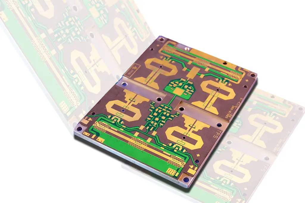
Simply put, it is a multilayer printed circuit board designed to carry signals from point to point at a specified frequency and speed. The signals are typically impedance controlled and on specific layers throughout the high-performance printed circuit board.
PCBs are usually produced on specialty laminate materials such as Rogers, Taconic, Isola, or Arlon to name a few. The board can be rigid, flex, or a combined rigid-flex and come in many different sizes, shapes, and thicknesses.
Material selection, layer stack-up, trace width and spacing, via placement, grounding, and signal integrity analysis are critical factors that should be considered while designing high-frequency PCBs. These PCBs are a type of electronic substrate that is designed to handle high-frequency signals. They are used in a variety of applications such as communication systems, radar systems, and medical equipment. Proper design of these PCBs will result in better signal quality and improved system performance.
High Frequency PCB Design Tips
- Material Selection
- Layer Stack-up
- Trace Width & Spacing
- Via Placement
- Grounding
- Signal Integrity
When you are designing printed circuit boards for your application, it is important to use materials that are going to give you the performance you need to make it a success. If you need something specifically for a high frequency, microwave or RF application, you will need to work with a manufacturer to get the laminates that will keep everything on track.
These laminates often require different types of b-stage/prepreg or bonding sheets to laminate them for multilayer PCB designs. The most commonly used is the Rogers RO4000 series. Talk with an expert at Benchuang Electronics to learn about the materials that are best for your PCBs.
Since then we have kept improving our experience of different base materials – and today we can process many different materials and even mixed buildups.
High frequency PCBs are typically used in radio and high speed digital applications such as 5G or 6G wireless communication, automotive radar sensors, aerospace, satellites and more. High frequency laminates provide lower attenuation and constant dielectric properties compared to PCBs of conventional FR4 materials. Benchuang Electronics has specialized in the manufacture of multilayer and HDI PCBs of high frequency dielectric materials.
Get started with High Frequency PCB
- Blind vias, buried vias, Ultra HDI PCB
- High frequency low loss PCB material
- TLY-5, RF35, RF-35TC, TSM-DS3, TLX-8, TLX-9 material
- RO4003, RO4350B, RO4835, RT/duroid 5870, RT/duroid 5880, RT/duroid 6002, TMM3, TMM4, TMM6, TMM10, TMM10i material