
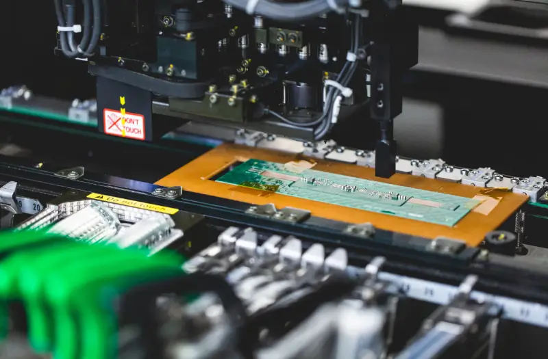
Printed circuit board fabrication and manufacturing has certainly evolved over the last few decades with the addition of new types of technology and manufacturing equipment. But one thing has remained the same — the process is often a complex and intricate one, and regardless of the type of PCB, proper manufacturing is essential to the board’s success and ability to function.
PCB Glossary of Terms
Before we begin, here are some of the most common terms used during the manufacturing process.
- Copper is a highly conductive element used to make the signal traces that conduct electricity.
- Etching refers to the action of removing unwanted excess copper from the copper layer.
- Lamination is the process of thermally laminating layers together. There are two main types — vacuum lamination and sequential lamination. Sequential lamination refers to the process of laminating two consecutive layers together. Vacuum lamination is a process in which air is extracted during the lamination process to prevent internal voiding in the circuit board or flex.
- Plating is a process where copper metal is electroplated onto the image of the PCB in order to plate through-holes.
- Laser drilling refers to the process of creating via-in-pad holes in the PCB.
- Silkscreen, known as a “silkscreen legend,” refers to the decals and reference designators in epoxy ink printed on a PCB. A silkscreen will help you recognize warning symbols and identify components and where they are to be placed. A silkscreen will also identify test points and manufacturer marks and more. The ink is typically white, and black may also be used at times when the substrate is white in color. The ink is digitally printed and doesn’t impact the function of a PCB, but it’s an equally important part of a PCB’s construction.
- Soldermask is a technique in which all parts of a circuit board are coated with epoxy except the contacts to be soldered, the gold-plated terminals of any card-edge connectors, and fiducial marks.
- Substrate refers to the base material used in a PCB.
- Via fill is a technique that completely closes a via, also known as a vertical interconnect access. A via is a plated-through hole in a PCB that is widely used to route a trace vertically in the board from one layer to another. Vias are typically filled with epoxy or another type of non-conductive material. A copper via electrolytic fill is used for blind vias.
Step-by-Step Guide Manufacturing Process for Multilayer PCBs
Now let’s go through each step of the PCB manufacturing process. It’s important to note that this guide pertains to all types of PCBs, but there may be slight variations with each step depending on the category of board.
- Define the substrate based on environmental and electrical requirements.
You first need to select what type of substrate material you will use for manufacturing. The choice of substrate and other materials will depend on the type of PCB and other parameters such as signal integrity,signal speed, and the environment in which it will be used. For example, single layer PCBs are made out of a single layer of substrate; one side is laminated with a layer of metal — typically copper. With double layer PCBs, both sides of the substrate have a metal layer. Multi-layer PCBs contain three or more copper conductive layers. A copper-clad substrate or polyimide-based film is used for flex circuits, and for rigid-flex circuits. Another substrate option includes Teflon (PTFE).


![Understanding PCB Costs & Pricing [Your Complete Guide]](https://hdicircuitboard.com/wp-content/uploads/elementor/thumbs/Understanding-PCB-Costs-Pricing-Your-Complete-Guide-qzzhe6mcaxuolkux3xalfktgavumi9y1aqfbs9bpv4.webp "Understanding PCB Costs & Pricing [Your Complete Guide]")
![Determining PCB Via Size [w Guidelines]](https://hdicircuitboard.com/wp-content/uploads/elementor/thumbs/Determining-PCB-Via-Size-w-Guidelines-qzzhe6mcaxuolkux3xalfktgavumi9y1aqfbs9bpv4.webp "Determining PCB Via Size [w Guidelines]")
![PCB Material Types Explained [Your Guide]](https://hdicircuitboard.com/wp-content/uploads/elementor/thumbs/PCB-Material-Types-Explained-Your-Guide-qzzhe6mcaxuolkux3xalfktgavumi9y1aqfbs9bpv4.webp "PCB Material Types Explained [Your Guide]")

