- AP 8515R, AP 9111R, AP 8525R, AP 9121R, AP 8535R, AP 9131R, AP 8545R, AP 9141R material
- PI (Polyimide Kapton) flexible pcb can be single-sided, double-sided, or multilayers with or without PTH and/or laser-defined micro-vias.
Custom Flexible PCB Solutions | Trusted Flex Circuit Board Manufacturer
Custom Flexible PCB & Bendable Circuit Board Options
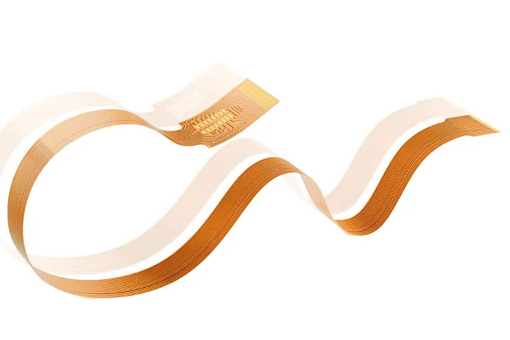
Single-Layer Flexible PCB (20μm Line Precision)
Flexible printed circuit boards (FPC) are offering the highest level of 3D miniaturization. Very low bending radii in combination with ultra-HDI (ultra-high density interconnect) are enabling our customers to build increasingly smaller and highly integrated devices. This technology is an enabler of small wearable devices as well it provides high signal density.
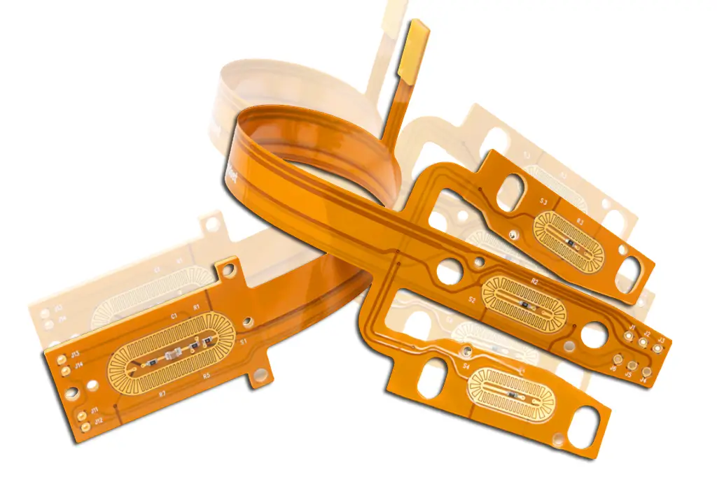
As an industry-experienced flexible PCB manufacturer, we craft tailored flexible circuit board solutions for automotive ADAS modules, medical diagnostic tools, and wearable tech. Our ISO 13485-accredited flex PCBs boast 20μm line precision, support up to 8-layer configurations, and endure extreme temperatures from -200℃ to 260℃—engineered specifically for mission-critical scenarios where failure isn’t an option. Our single-layer bendable circuit boards, ranging from 0.05mm to 0.2mm thick, excel at simple signal transmission in wearables like fitness trackers. We guarantee 99.9% trace width accuracy, and offer optional edge plating to boost connector contact reliability in high-vibration environments.
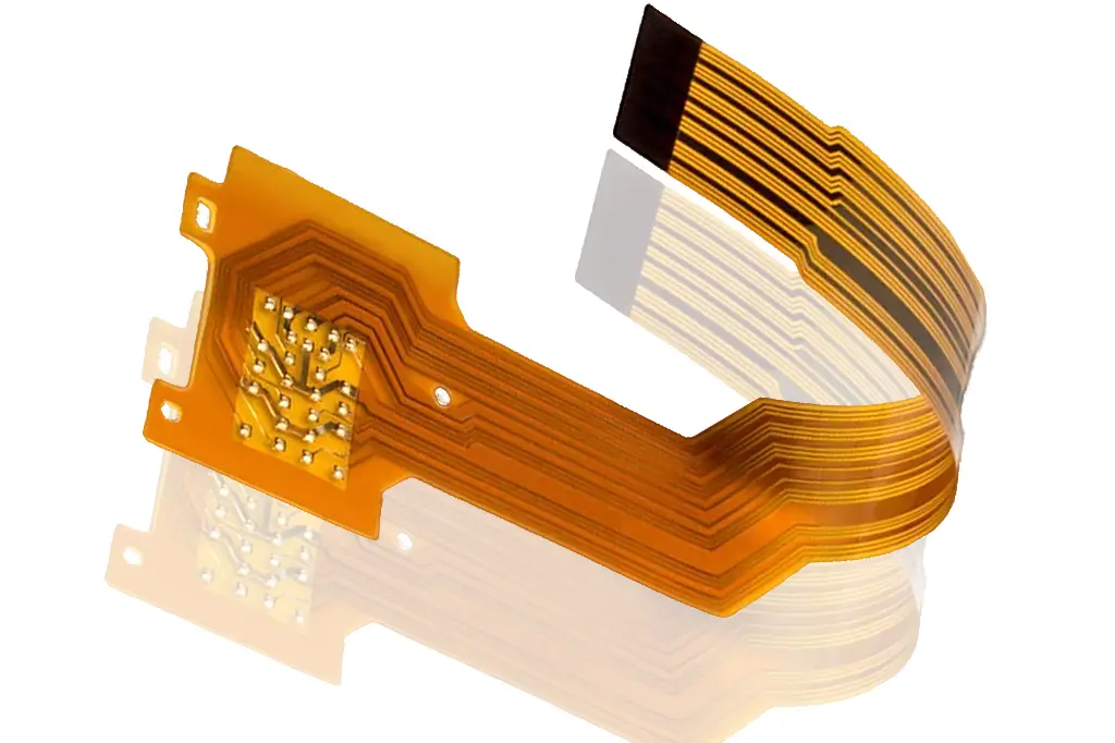
Multi-Layer Flexible Printed Circuit (8 Layers Max)
Our multi-layer flexible printed circuits top out at 8 layers, designed for high-density interconnect demands in aerospace avionics and satellite communication systems. We integrate dedicated internal ground planes to cut electromagnetic interference (EMI) by 40% versus single-layer designs, achieving ±0.02mm interlayer alignment via laser registration—critical for high-pin-count component integration. These flex circuits utilize blind/buried vias (0.1mm diameter) for compact signal routing, eliminating the bulk of traditional through-holes and fitting tight installation spaces in precision equipment.
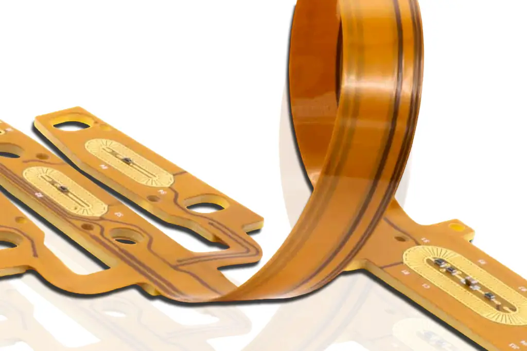
Rigid-Flex Flexible Circuit Board (Custom Stackup)
Our rigid-flex flexible circuit boards blend the flexibility of PI-based circuits (for dynamic components) with rigid FR-4 sections (for stable chip mounting). This hybrid design removes the need for extra connectors, simplifying assembly and slashing failure points in automotive BMS and portable medical monitors. We customize stackups to client needs: rigid sections use 1oz–2oz copper for power delivery, flex sections employ 1oz PI copper for bending resilience, with a 1mm minimum flex-rigid transition radius to avoid stress concentration.
High-Grade Flexible Printed Circuit Board Substrates
PI Substrates for High-Temp Flexible PCB (-200℃~260℃)
We source top-tier substrates for flexible printed circuits—Polyimide (PI), Liquid Crystal Polymer (LCP), and Polyester (PET)—all fully RoHS 3.0 and REACH compliant to ensure global market access. Our PI flexible PCB substrates, sourced from DuPont Kapton® FN, handle temperatures from -200℃ to 260℃ and resist harsh chemicals like automotive fluids and aerospace hydraulic oils, making them ideal for under-hood BMS systems. We pair 12μm–70μm electrodeposited copper foil with 25μm–75μm PI coverlay to enhance bending durability, supporting 100,000+ flex cycles in repetitive-motion applications.
LCP Substrates for High-Freq Flexible Circuit
Our LCP substrates enable high-frequency signal transmission up to 60GHz with minimal insertion loss (≤0.3dB/inch at 24GHz), perfect for 5G mmWave transceivers and high-speed data devices (USB 4.0, Thunderbolt). These flexible circuits feature a stable dielectric constant (Dk=3.0±0.05) and ultra-low dissipation factor (Df≤0.002), ensuring signal integrity at high speeds. They’re laser-drillable for 0.1mm microvias, enabling compact designs in space-constrained telecom equipment, and their low CTE (6ppm/℃) prevents warpage during reflow soldering.
Cost-Effective PET Flexible PCB Substrates
For budget-conscious consumer electronics (operating at ≤1GHz), our PET flexible PCB substrates deliver reliable performance with a 1mm minimum bending radius and 20kV/mm dielectric strength. We use 50μm–125μm PET base material paired with 18μm–35μm copper foil, ideal for smart watch straps, remote control circuits, and low-power sensors. These flex PCBs strike a balance between cost and functionality, supporting mass production of consumer gadgets without compromising on basic reliability—our typical batch yield exceeds 99.5%.
Precision Flexible PCB Fabrication Processes
Laser Drilling for Flexible PCB
Our flexible PCB fabrication relies on UV laser drilling with ±25μm positioning accuracy, creating microvias as small as 30μm. This precision avoids the vibration-induced via voids common with mechanical drilling, keeping void rates ≤0.3%—critical for medical implantable devices and aerospace radar modules where even tiny defects can cause failure. We also offer via-in-pad technology with chemical planarization, ensuring surface flatness ≤10μm for reliable assembly of fine-pitch BGA components (0.2mm pitch).
Uniform Plating for Flex Circuit Board Durability
We use pulse plating technology for copper traces (12μm–70μm thickness), ensuring consistent conductivity and bending resilience across every flex circuit board. For RF signal pads, optional gold plating (≥0.05μm) enhances solderability and resists oxidation, while ENIG plating is used for digital layers to optimize cost. All plating processes adhere to IPC-6013 standards, and every batch undergoes peel strength testing (≥1.2N/mm) to confirm bond integrity between copper and substrate.
100% AOI Testing for Flexible PCB Reliability
Every flexible PCB goes through 100% automated optical inspection (AOI) with 5μm resolution, catching open circuits, short circuits, trace defects, and solder mask gaps that manual inspections miss. For aerospace and medical-grade products, we add thermal shock testing (-55℃~125℃, 1000 cycles) and humidity testing (85℃/85% RH, 1000h) to validate environmental resilience. High-reliability orders include cross-sectional via analysis and full test reports, ready for regulatory submissions.
Industry-Tailored Flexible Circuit Solutions
Automotive Flexible PCB for BMS & ADAS Systems
Our automotive flexible PCBs for BMS and ADAS systems meet AEC-Q200 standards, withstanding 20G vibration (10Hz~2000Hz) and operating temperatures from -40℃ to 125℃—ideal for electric vehicle applications. We reinforce bend zones with extra PI coverlay to support 100,000+ flex cycles, and use flame-retardant PI substrates (UL 94V-0) to reduce fire risk. Mass production achieves 99.9% first-pass yield, helping automotive OEMs meet NCAP 5-star safety standards for collision avoidance.
Medical Flexible Circuit Board
Our ISO 13485-certified medical flexible circuit boards use USP Class VI biocompatible PI substrates, safe for implantable devices, ECG monitors, and diagnostic tools with ≤10mW standby current. We manufacture these in Class 10000 cleanrooms to eliminate particulate contamination, and maintain full batch traceability from raw material to delivery. The boards support sterilization via autoclave or gamma radiation without performance degradation, meeting FDA requirements for medical electronics.
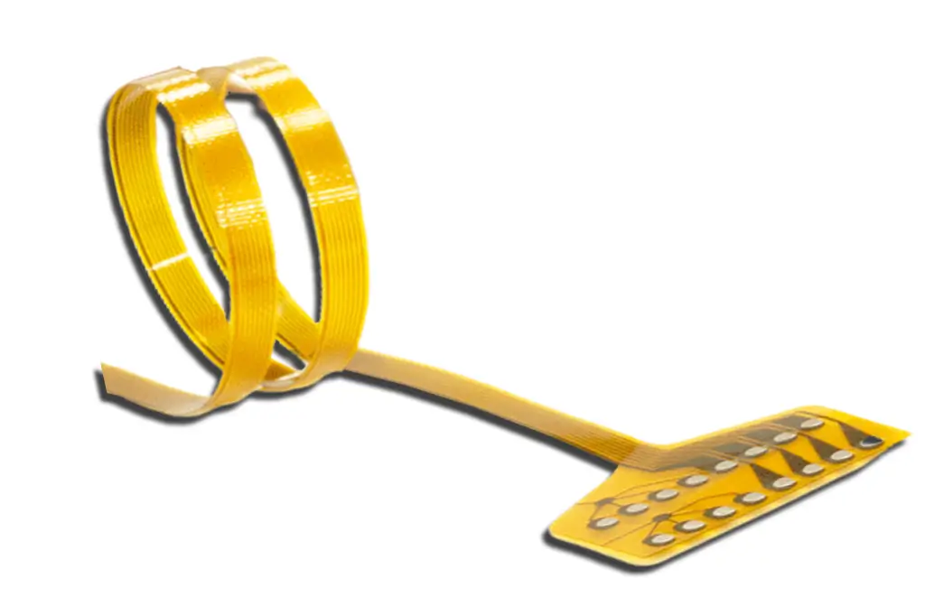
Flexible PCB for Wearables & Foldable Devices
Our flexible PCBs for wearables and foldable devices feature ultra-thin designs (0.055mm minimum thickness) and support 100,000+ bending cycles—critical for foldable smartphones and smart watch straps. We use PI-PET hybrid substrates to balance light weight and durability, with 3mil/3mil trace width/spacing for compact sensor integration. Custom shapes (curved, irregular) are available to fit unique product form factors, and we optimize designs to minimize power consumption for battery-powered wearables.
ISO-Certified Flex Circuit Board Manufacturer Services
Free DFM for Flexible Printed Circuit Design
As a leading flex circuit board manufacturer, we offer free DFM (Design for Manufacturing) consulting for flexible printed circuit designs. Our engineering team validates material compatibility, trace feasibility, and stackup optimization, cutting design cycles by 30%. We use 3D electromagnetic simulation to verify impedance control (50Ω/75Ω, ±3% tolerance) before prototyping, eliminating costly trial-and-error and ensuring designs are production-ready from day one.
ISO 13485 & UL Certified Flex PCB Manufacturer
Our facilities hold ISO 13485 (medical), ISO 9001:2015, UL (File No. E362589), and CE certifications, ensuring all flex PCBs meet regional regulatory requirements—FDA for medical devices, FCC for telecom, and MIL-STD-883H for aerospace. We provide complete compliance documentation with every batch, simplifying clients’ regulatory submissions and market access processes.
24/7 Technical Support for Flex Circuit Clients
We offer 24/7 technical support for global flex circuit clients via phone, email, and video conferencing, with dedicated account managers assigned to bulk orders. All flexible PCB products come with a 12-month warranty covering manufacturing defects (e.g., poor plating, delamination).
Flexible Circuit Board Capabilities:
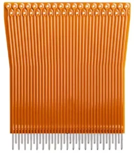
- Single Sided Flex pcb or double sided flex pcb
- Multilayer flex pcb from 3 to 16 layers
- 1/4 oz – 7 oz copper
- Sizes from 2 to 40 feet in length, longer upon request
- Width maximum of 20″
- Adhesive-based and adhesiveless constructions
- PI film substrates
- Low-cost, Roll-to-Roll manufacturing
- Fine line copper etch conductors
- Photo imageable solder masks
- Laminated coverlay dielectrics
-
Surface finishes include:
- OSP
- Immersion Silver
- Immersion Tin
- Electroplated Nickel Gold
- ENIG
- ENEPIG -
Various support materials can be selectively added, including:
- Metal heatsinks
- Film stiffeners
- Polyimide, Aluminum, Stainless Steel
- Release Films
- EMI shielding
- Molded plastic assemblies
Flex Circuit Board Bending Radius
The bend radius calculation rule is explained in IPC-2223B:
With as main objective to keep constraints lower than the FPCB copper elongation limit
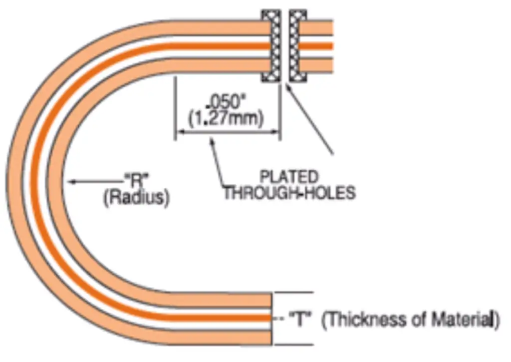
Flex Circuit PCB Minimum Bending Radius
EB= % Copper Elongation desired
Rolled Annealed max. ≤16%
Electro-deposited max. ≤11%
Flex to install applications ≈3%
Dynamic flex applications ≈0.3%
Disk drive applications ≈0.1%
R = radius of fold
c = copper thickness
D = dielectric thickness with adhesive
d = flexible clad dielectrics thickness
(Central “adhesive+PI+adhesive” for double side)
Case of single-sided flexible pcb with coverlay calculation
R = c/2 x [(100-EB)/EB] – D
Case of double-sided flexible pcb with coverlay calculation
R = (d/2 + c) x [(100-EB)/EB] – D
How To Calculate Flex Circuit Board Minimum Bend Radius
- Rmin=6xFPC_thickness
- Rmin=10xFPC_thickness for double side.
- Rmin=15xFPC_thickness for multilayer side.
- Rmin=25xFPC_thickness for dynamic.
Flexible PCB Board Materials
Flex PCB materials need to support multiple design and operational goals: static or dynamic flexing, the ability to pass through standard assembly processes, and support for simple fabrication procedures with high yield. Flex PCB materials may seem exotic at first, but a relatively small material set is used to produce flex and rigid-flex PCBs at high volume.
Substrate and Coverlay Films
The base material used in most common rigid printed circuit boards is woven fiberglass impregnated in epoxy resin. It’s a fabric, and although we term these “rigid” if you take a single laminate layer they have a reasonable amount of elasticity. It’s the cured epoxy that makes the board more rigid. Because of the use of epoxy resins, they are often referred to as organic rigid printed circuit boards. This is not flexible enough for many applications though for simple assemblies where there’s not going to be constant movement it can be suitable.
The most common material choice used as a flex PCB substrate is polyimide. This material is very flexible, very tough, and incredibly heat resistant.
For the majority of flex circuit applications, more flexible plastic than the usual network epoxy resin is needed. The most common choice is polyimide, because it’s very flexible, very tough (you can’t tear or noticeably stretch it by hand, making it tolerant of product assembly processes), and also incredibly heat resistant. This makes it highly tolerant of multiple solder reflow cycles, and reasonably stable in expansion and contraction due to temperature fluctuations.
Polyester (PET) is another commonly used flex-circuit material, but it’s not tolerant enough of high temperatures to survive soldering. I have seen this used in very low-cost electronics where the flexible part had printed conductors (where the PET could not handle the heat of lamination), and needless to say nothing was soldered to it – rather, contact was made by crude pressure with an isotropic conductive elastomer.
The display in the product in question (a clock radio) never really worked too well due to the low quality of the flex circuit connection. So for rigid-flex, we’ll assume we’re sticking to the PI film. (Other materials are available but not often used).
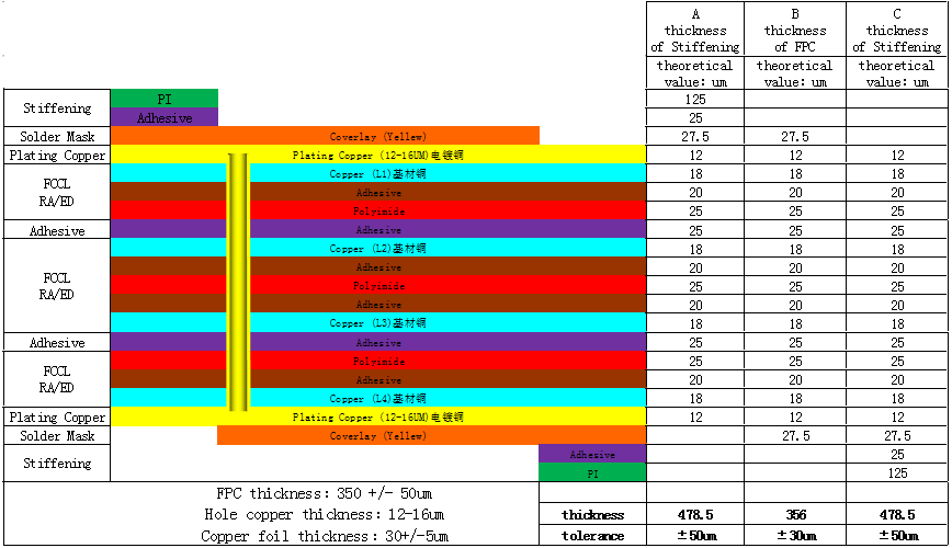
PI and PET films, as well as thin flexible-epoxy-and-glass-fiber cores, form common substrates for flex circuits. The circuits must then use additional films (usually PI or PET, sometimes flexible solder mask ink) for coverlay. Coverlay insulates the outer surface conductors and protects from corrosion and damage, in the same way a solder mask does on the rigid board. Thicknesses of PI and PET films range from ⅓ mil to 3 mils, with 1 or 2 mils being typical. Glass fiber and epoxy substrates are sensibly thicker, ranging from 2 mils to 4 mils.
DuPont AP Adhesiveless flexible printed circuit board Materials
| Product | KKapton® Thickness | Copper Thickness |
|---|---|---|
| AP8515 | .001″ | 1/2 ounce (.0007″) |
| AP9111 | .001″ | 1 ounce (.00014″) |
| AP9212 | .001″ | 2 ounce (.00028″) |
| AP8525 | .002″ | 1/2 ounce (.0007″) |
| AP9121 | .002″ | 1 ounce (.00014″) |
| AP9222 | .002″ | 2 ounce (.00028″) |
| AP8535 | .003″ | 1/2 ounce (.0007″) |
| AP9131 | .003″ | 1 ounce (.00014″) |
| AP9232 | .003″ | 2 ounce (.00028″) |
| AP8545 | .004″ | 1/2 ounce (.0007″) |
| AP9141 | .004″ | 1 ounce (.00014″) |
| AP9242 | .004″ | 2 ounce (.00028″) |
| AP8555 | .005″ | 1/2 ounce (.0007″) |
| AP9151 | .005″ | 1 ounce (.00014″) |
| AP9252 | .005″ | 2 ounce (.00028″) |
| AP8565 | .006″ | 1/2 ounce (.0007″) |
| AP9161 | .006″ | 1 ounce (.00014″) |
| AP9262 | .006″ | 2 ounce (.00028″) |
Bendable Circuit Board Structures
Flexible circuit applications typically include designs where the circuit wraps around other electrical subsystems or rests against the inside of an instrument enclosure. Therefore, the material options commonly available for these purposes have specific mechanical, thermal and chemical properties. So, it’s possible to adapt this layer depending on the desired performances (mechanical strength, temperature resistance, bending…).
Single Sided Flex PCB
The single layer flexible printed wiring boards have only one conductive layer (single sided conductor pattern) with coverlayer and no plating in the through holes. In addition, the design may contain shields, to improve a thermal dissipation, or stiffeners.
Coverlayer can be coverlay or covercoat or even both when used on different areas of same FPCB
Double Sided Flex PCB
The double layer flexible printed wiring boards present conductor patterns on both sides of the printed wiring board. In addition, the design of the printed wiring board may require:
That the holes through the base material be plated to electrically connect together the conductor patterns on both sides, Shields can be used to improve thermal dissipation and stiffeners can be used to stiffen the board.
Coverlayer can be coverlay or covercoat or even both when used on different areas of same FPCB. Double layer with copper area at the bottom is better to dissipate the heat coming from top components mainly LEDs. This improves also the CEM when this area is set to GND.
Multilayer Flex PCB
This type of flexible printed wiring boards are multilayered (with three or more conductor layers) and require plated-through holes. We could use through vias, buried vias and blind vias.
4 Layer Flex PCB
A four-layer flex circuit has four conductive copper layers.
For dynamic applications, the bend radius should be 100 times the finished board thickness.
If there are no traces in the bend region, insert circular cutouts with radii greater than 30 mils to minimize the amount of material that needs to be deformed and increase flexibility.
Avoid plated through holes and component placement within the bend area. Place plated through holes at least 20 mils away from the bend area.
Flex PCB Fabrication
Flexible LED PCB
LED strips are basically individual circuit boards with electrical interconnections. Flexible PCBs comprise most of such strips, with SMD LEDs mounted on them. In other words, the flexible PCB forms the substrate on which manufacturers mount SMD LEDs. Besides providing a flexible structure, the substrate material also helps in dissipating the heat generated by individual LEDs when operating.
The high flexibility of the LED strips allows stringing up the strip into any shape. LED strips are commonly available in 5-meter long reels.
Thermal Management Flexible LED Circuits transmit heat away from critical components (or operating areas) to ancillary spaces using one or more of the following: metal heatsinks , metallic cores (e.g., aluminum, Cu), thermally conductive dielectrics (Stabl-Cor, graphene), or heavy copper plane layers.
Flexible LEDs provide better heat transfer and increased flexibility that reduces soldering as well as a palletized tab-routed array that allows customer to easily assemble multiple pieces simultaneously during mass assembly process.
Transparent Flexible PCB
Different PCB specifications apply to new electrical and electronic equipment. Flexible PCBs are frequently made using polyamide, PEEK (polyether ether ketone), or a transparent conductive polyester sheet as the substrate. As a result, it is common to see translucent ceramics boards, transparent circuit boards, and aluminum PCBs installed inside them, keeping the idea of a clear board in mind. The market has long featured transparent PCBs.
Flexible PCBs (FPCs) built of PET thin film are transparent. PET materials are available in clear white, light blue, green, and a few different colors. Clear FPCs can only be distinguished from traditional flexible PCBs by using transparent PET materials. In certain transparent flexible PCBs, you can see the electrical traces, and pads are visible. Some transparent flexible PCBs have completely transparent conductive traces. The circuit is secured between two translucent materials using an inventive manufacturing technique, rendering it imperceptible from the outside.
Technical specifications
- Transparency might be anything between 94.36% and 100%.
- The number of layers on the transparent circuit board might be between one and 10.
- Between 0.1 mm and 0.6 mm is the thickness of the final transparent flex PCB.
- The range of copper thickness is 17.5 mm to 70 mm.
- The surface finish incorporates a variety of ingredients, including immersion tin, immersion silver, ENIG, OSP, and ENEPIG.
- The laser blind hole must be at least 0.075 mm in diameter.
- The mechanical drilling hole must be at least 0.1 mm in diameter.
- The required line width is 0.035 mm.
- Line spacing must be at least 0.035 mm.
- A blind hole can have an aspect ratio as high as 0.8.
- The interlayer alignment must be at least 0.05 mm.
- The heat tolerance for soldering may increase to 260 °C in 5 seconds.
- The required adhesive strength is 490 N/m.
- 300 °C is the maximum temperature at which glass transitions.
- The operating temperature ranges from -25 to +75 degrees Celsius.
Sculptured Flex Circuits
Sculpted flexible circuits have sculpted pins, which are made as a through-hole connector. Sculptured terminal pins are built-in and extended beyond the boundary of the polyimide base material. These pins are plugged into a series of holes in a PCB and then soldered. This circuit design, is also able to be soldered to a series of surface mount pads. Sculpted flex circuits are often chosen to eliminate the need and cost of a ZIF connector.
Sculptured Jumper
These sculptured jumpers are special in that they have connection pieces made from thick, rigid copper that are fully-integrated extensions of the conductors from the flexible part of the jumper, ensuring maximum reliability of connections.
Sculptured jumpers use a rigid PCB produced with a thick sheet of copper (generally 250 µm thick, though there are other options) with reduced thickness in areas that need to be flexible. At the same time, the full thickness of the copper is maintained for high-power conductors and terminals. An insulating film is then applied to each surface.
Sculptured Flex Circuit Features
- Fingers are an integral part of the conductor patterns
- Customized for any pitch & configuration of mating board
- Straight or formed contacts available
- Unsupported termination traces
- Terminal point is thicker & can be directly used as a connector
- Eliminates a mechanical connection point & makes the connection more reliable
Flex PCB Supplier
Thick Copper Flex PCB
Available in different thicknesses of copper (up to 500 µm), differential copper PCBs can meet your most specific needs for various mechanical and electrical characteristics. Using a differential etching process, we can reduce the thickness of conductors in areas that must be flexible while maintaining the full original thickness of the copper for high-power conductors and terminals. An insulating film is then applied to each surface. The copper remains accessible on both faces in the selected areas.
Ultra Fine Line Flex PCB
Smaller devices require smaller circuits, and in many cases, those circuits must be flexible enough to bend during use. Unlike rigid printed circuit boards, flexible circuits carry their components on flexible plastic substrates that allow movement during use.
Designing and building a high-density flex circuit that can withstand extreme temperatures, hold up under repeated use, and have lines and spaces as small as 25μm isn’t the easiest of tasks. And, accomplishing this task in over 20 days or less with lot sizes as small as one unit requires a tremendous amount of experience and teamwork.
High density interconnect (HDI) PCB technology, including fine lines and spaces (1.5 mil and below) is a key enabling technology for the next generation of portable electronic devices. This technology offers many advantages over conventional technologies, including circuit board size reduction, increased routing, and lower fabrication costs.
Fine Line Flex PCB Highlight
- Adhesiveless construction resulting in more rugged, thinner, lighter and more flexible circuits
- Higher density circuits: trace and space capabilities down to 1.5 mil
- Microvia sizes down to .002″ diameter for high density, 2-layer flex circuits
- Selective plating of gold and tin leads enables multiple attachment methods on the same All-Polyimide flex circuits
- Alternate circuit layer materials such as beryllium, copper, stainless steel, and nickel can be used for optimum performance in unique applications
- Leaded and Lead-Free Assemblies
Ultra Thin Flexible PCB
New approaches are needed to meet the increasing demand for smaller and thinner electronic devices. Both rigid and flexible ultra-thin base materials for PCBs can fill this need by enabling higher-density designs with enhanced miniaturization in the Z direction, leaving more space for other components or reducing the overall thickness of the device. Because these materials require specific design approaches and fabrication technology, it’s important to collaborate with a PCB manufacturer that has advanced engineering services to ensure a PCB design that is compact, cost-effective and reliable.
Benchuang Electronics provides our customers with Ultra-Thin Flexible Printed Circuit Boards using 3 µm Copper on 25 µm polyimide or 18 µm copper on 12.5 µm polyimide.
Two-layer Flexible Printed Circuit Boards as thin as 0.055mm +/-.03mm thick. When space and weight are critical for products for the wearable and medical markets among others. Special design parameters are called for when building this technology and the key process components must be used throughout the fabrication process.
This cutting-edge technology requires special expertise and processes including photolithography (Direct Imaging) to create very fine-line copper traces and spaces. Tightly controlled etching and plating processes as well as testing and inspection.
Producing ultra-thin flex circuits with such specific requirements requires specialized equipment, materials, and expertise. Strict process control parameters are needed to assure that all quality and technology requirements are met throughout the entire process of the Flex Printed Circuit.
HDI Flex PCB
Micro Vias
Microvias are holes through one or more layers of a flexible circuit board made of alternating insulating and conducting layers of material. These materials are often copper sheet (1/2 oz typically) and an epoxy/fiberglass blend in thin sheets (.001-.002” thick). The laser drilling tool will create a via from the top layer down to a copper catch pad below which will be plated to form an electrical connection between conducting layers.
The drilling, and subsequent plating works best when the diameter of the via is equal to or greater than the depth of the via (a 1:1 ratio is ideal). Benchuang Electronics generates vias in the range of .003” to .008” (.075-.100mm) with capability to produce smaller and larger sizes.
High Density Interconnect
Running out of real estate with conventional feature sizes? Benchuang Electronics High Density Interconnect (HDI) flex circuits can improve electrical performance and consistency by using vias as small as 50 microns or 9-micron copper to increase density in a small electronic package.
High Density Interconnect (HDI) flex circuits offer designers the same benefits of flex circuits—smaller, more reliable products—except at a higher level. In addition to the design benefits of HDIs and microvias listed below, HDI circuits give you more design, layout and construction options helping you finish your design in less time.
Large Format Flex PCB
Long Flex PCB
Benchuang Electronics specialises in designing and manufacturing large-format PCBs for many different uses and configurations.
We are able to produce flexible PCBs that are several metres long thanks to our mastery of the roll-to-roll manufacturing process.
These flexible PCBs, much larger than standard-sized PCBs and without any real limit on size, offer a major advantage. They allow you to produce a single piece that includes all functional parts along with all necessary connectors, whereas a traditional design would require the combination of one or more rigid PCBs with wired connections.
Benchuang Electronics has the unique capability to provide our customers with extra-long FPC and PCBs as long as 15 M (50 feet), making us one of the few suppliers who can provide boards this size.
Benchuang Electronics assures that the extra-long Flex Printed Circuits that will meet all of the customers’ products’ dimensional requirements including being able to assure proper flatness and shrinkage tolerances as well as making sure that the product will fit properly into the customers’ end product.
Flex Circuit PCB Stiffener Requirements
Flexible PCB stiffener requirements fall under the following usage categories:
- Rigidizing connector areas for stress relief of larger connectors or repeated insertions of the connector
- ZIF (Zero Insertion Force) Thickness Requirements
- Localized Bend Constraint(s)
- Creating a flat surface for the placement of SMT pads and components
- Minimizing component stress
- Managing heat dissipation (aluminum and steel)
- Make the array rigid enough to run through the automated assembly processes without a fixture
Flexible Printed Circuit Stiffener Application
Flexible PCB stiffener requirements fall in the following usage categories:
- Rigidizing Component / Connector areas
- ZIF (Zero Insertion Force) Thickness Requirements
- Localized Bend Constraint(s)
Component / Connector Stiffeners
Essentially, they create a rigid area where components and connectors are attached. They also protect solder joints by ensuring the flex doesn’t bend in the component area.
ZIF Stiffeners
They ensure that the thickness is increased at contact fingers to meet specific ZIF connector specifications.
Localized Bend Constraints
They restrict bend areas to specific locations in a flex design.
Flexible Printed Circuit Board Manufacturer
Benchuang Electronics has firmly established itself as a leading and reliable manufacturer of flexible printed circuit boards (Flex PCB). With a commitment to excellence and a focus on quality, Benchuang Electronics has consistently delivers innovative and precision-engineered Flex PCB solutions to meet the diverse needs of its clients.
Our dedication to maintaining the highest standards in manufacturing is reflected in the durability, reliability, and performance of our flexible circuit boards. Whether it’s for medical devices, aerospace applications, or industrial electronics, Benchuang Electronics stands out as a trusted partner, providing top-notch rigid flex PCB solutions that exemplify durability, flexibility, and unparalleled quality in the ever-evolving field of electronics manufacturing.
Get started with Flexible PCB
- Single-sided, double-sided, multilayer, HDI flex pcb
- Large-format flex pcb, high temperature flex pcb
- Thick copper flex PCB, sculptured flex PCB
- AP 8515R, AP 9111R, AP 8525R, AP 9121R, AP 8535R, AP 9131R, AP 8545R, AP 9141R material