
Flexible PCB layer stackup design requires precise material selection, symmetric layer arrangement, and strict adherence to IPC-2223 and IPC-6012 standards to ensure mechanical flexibility, signal integrity, and long-term reliability. This guide details single-sided, double-sided, multilayer, and rigid-flex stackups with critical parameters including layer thickness, copper weight, bend radius, and impedance control for optimal performance in dynamic applications.
Learn more about: What is a Flexible PCB? A Complete Guide for Beginners
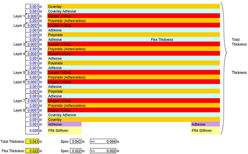
What is Flexible PCB Layer Stackup
Core Definition & Purpose
- Structured arrangement of conductive copper layers, dielectric substrates, adhesives, and protective films
- Establishes electrical performance, mechanical flexibility, thermal stability, and manufacturability
- Governs impedance control, signal propagation, and bend cycle performance
- Complies with IPC-4203 (flex materials) and IPC-6012 (qualification) standards
Fundamental Stackup Principles
- Symmetric construction: Balances thermal/mechanical stress, prevents warping (IPC-2223)
- Continuous reference planes: Ensures impedance stability and signal integrity
- Minimum layer count: Optimizes cost while meeting electrical requirements
- Material compatibility: Matches dielectric constants (Dk) and thermal coefficients
Standard Material Stackup Components
Base Dielectric Materials
- Polyimide (PI): 12.5μm, 25μm, 50μm standard thickness; Dk=3.5±0.1; temp range -55°C to +150°C
- Liquid Crystal Polymer (LCP): 25μm, 50μm; Dk=3.0±0.05; ultra-low loss for high-frequency
- Polyester (PET): 25μm-100μm; cost-effective; limited to -20°C to +80°C
- Adhesives: 12.5μm-25μm modified acrylic or epoxy; low-flow (<10μm squeeze-out)
Conductive & Protective Layers
- Copper foil: 5μm (1/4oz), 9μm (1/3oz), 12μm (1/2oz), 18μm (1oz), 35μm (2oz)
- Rolled Annealed (RA): Superior flexibility (>10,000 flex cycles)
- Electrodeposited (ED): Lower cost; adequate for static applications
- Coverlay: 25μm-50μm polyimide with adhesive; protects flex circuits
- Solder mask: 10μm-18μm LPI; for rigid sections or low-flex applications
- Stiffeners: FR-4, stainless steel, or PET; 0.1mm-0.5mm thickness for component mounting
Flex PCB Material Properties Comparison
| Material Type | Temperature Range | Dk Value | Flex Performance | Cost Factor |
|---|---|---|---|---|
| Standard PI | -55°C to +150°C | 3.5±0.1 | Excellent | 1.0 |
| LCP | -55°C to +125°C | 3.0±0.05 | Good | 1.8 |
| PET | -20°C to +80°C | 3.2±0.2 | Fair | 0.6 |
| RA Copper | -60°C to +260°C | N/A | Superior | 1.3 |
| ED Copper | -60°C to +260°C | N/A | Good | 1.0 |
Common Flexible PCB Stackup Configurations
Single-Sided & Double-Sided Flex
Single-Sided Flex (1-layer)
- Structure: Coverlay → Copper (12.5μm) → PI (25μm) → Coverlay
- Total thickness: 50μm-75μm
- Minimum line/space: 50μm/50μm
- Applications: Simple sensors, low-count interconnects
- Bend radius: Static ≥6× thickness; Dynamic ≥10× thickness
Double-Sided Flex (2-layer)
- Structure: Coverlay → Cu (12μm) → PI (25μm) → Adhesive (12.5μm) → PI (25μm) → Cu (12μm) → Coverlay
- Total thickness: 100μm-125μm
- Interconnection: Plated Through Holes (PTH) 0.2mm-0.3mm diameter
- Impedance: 50Ω±5% (microstrip); controlled via dielectric thickness
- Bend performance: >5,000 cycles with RA copper
Multilayer Flex (4-10 Layers)
4-Layer Standard Stackup
- Coverlay (25μm)
- Signal Layer (12μm Cu)
- PI Dielectric (25μm)
- GND Plane (18μm Cu)
- Adhesive (12.5μm low-flow)
- Power Plane (18μm Cu)
- PI Dielectric (25μm)
- Signal Layer (12μm Cu)
- Coverlay (25μm)
- Total thickness: 175μm-200μm
- Impedance: 50Ω stripline; controlled to ±5%
- Bend radius: ≥12× total thickness for dynamic applications
6-Layer High-Speed Stackup
- Alternating signal/GND layers for optimal shielding
- Signal layers separated by ground planes (≤0.2mm spacing)
- Power planes adjacent to ground planes for decoupling
- Minimum bend radius: ≥15× thickness
- Suitable for GHz-range signals with controlled impedance
Rigid-Flex PCB Stackup
Standard 4-Layer Rigid-Flex PCB
- Rigid sections: FR-4 core (0.2mm-0.4mm) with 18μm Cu
- Flex sections: 2-layer PI (25μm each) with 12μm Cu
- Transition: Tapered rigid-framed structure; 5mm transition zone minimum
- Total thickness: Rigid=0.6mm-1.0mm; Flex=0.1mm-0.15mm
- Registration tolerance: ±25μm layer-to-layer
Key Rigid-Flex Features
- Stiffeners in component mounting areas (0.2mm-0.5mm thickness)
- Coverlay only on flex sections; solder mask on rigid areas
- Bend radius: ≥10× flex thickness in dynamic zones
- Complies with IPC-2223 Section 9 (rigid-flex design criteria)
Learn more about: Rigid-Flex PCB Manufacturing Process Step by Step
Flexible PCB Stackup Types Comparison
| Stackup Type | Typical Thickness | Min Bend Radius | Max Layers | Best Application |
|---|---|---|---|---|
| Single-Sided Flex | 50-75μm | 6× thickness | 1 | Simple interconnects |
| Double-Sided Flex | 100-125μm | 8× thickness | 2 | Moderate complexity |
| 4-Layer Flex | 175-200μm | 12× thickness | 4 | Impedance control |
| 6-10 Layer Flex | 250-500μm | 15× thickness | 10 | High-speed systems |
| Standard Rigid-Flex | 0.6-1.0mm (rigid) | 10× flex thickness | 8 | 3D packaging |
Key Design Considerations
Layer Selection & Symmetry
- Even layer preference: 2,4,6 layers for balanced stress distribution
- Symmetric thickness: Top/bottom dielectric thickness matched within 5%
- Copper balance: Total copper weight balanced top/bottom (±10%)
- Layer ordering: Signal layers adjacent to reference planes (≤0.2mm spacing)
- Unbalanced stackup risk: >0.5% warpage after lamination; 30% higher failure rate
Bending Area Optimization
- Dynamic bend zones: Minimum 5mm straight section before bending
- No components in bend areas: 2mm clearance required
- Trace orientation: Perpendicular to bend axis; minimum 0.2mm width
- Strain relief: Tapered copper width reduction at bend entry points
- IPC standard: Bend radius ≥6× static; ≥10× dynamic (IPC-2223)
Transition Area Design
- Gradual transition: 45° angles or curved interfaces (no sharp corners)
- Minimum length: 5mm transition zone between rigid/flex
- Staggered layer termination: Prevents stress concentration
- Adhesive control: Low-flow prepreg (≤10μm squeeze-out) in transitions
- Testing: Thermal cycling (-40°C to +125°C) without delamination
Key Design Guidelines for Flexible PCB Stackups
Electrical Performance Parameters
- Impedance control: 50Ω single-ended; 90Ω/100Ω differential (±5%)
- Dielectric thickness: 25μm±2μm for controlled impedance
- Minimum line/space: 40μm/40μm (12μm Cu); 30μm/30μm (5μm Cu)
- Via specifications: 0.2mm-0.3mm diameter; 0.4mm pitch minimum
- Insulation resistance: >100MΩ at 500VDC (IPC-6012 Class 3)
Mechanical Reliability Standards
- Bend cycle performance:
- Static: >1,000 cycles without failure
- Dynamic: >5,000 cycles (RA copper); >10,000 cycles (ultra-thin Cu)
- Peel strength: ≥1.0N/mm (Cu to PI); ≥0.8N/mm (coverlay to Cu)
- Thermal stability: 260°C for 10s (3× reflow) without blistering
- Moisture resistance: <0.1% weight gain after 85°C/85%RH/1000h
Common Mistakes to Avoid
Layer Structure Errors
- Asymmetric stackups: Causes warping (>0.5%) and internal stress
- Insufficient reference planes: Poor signal integrity and EMI performance
- Mismatched materials: Different CTE causes delamination during thermal cycling
- Excessive layer count: Unnecessary cost and reduced flexibility
- Non-standard thickness: Manufacturing difficulty and yield issues
Copper & Via Design Errors
- Excessive copper thickness: >18μm in dynamic flex zones (cracking risk)
- PTH in bend areas: Stress concentration points; 3× diameter clearance required
- Unbalanced copper distribution: >10% weight difference causes curling
- Inadequate web width: <0.2mm between features (breakage risk)
- Missing teardrops: At via connections; reduces stress by 40%
Material & Processing Misapplications
- Using PET in high temp: >80°C applications causes material failure
- Insufficient coverlay adhesion: <0.8N/mm peel strength leads to delamination
- Standard solder mask on flex: Cracks after <1,000 cycles
- Inadequate adhesive control: >10μm squeeze-out causes short circuits
- Ignoring Dk variations: >5% tolerance results in impedance mismatch
Core Technical Parameters
- Base materials: Polyimide (25μm, Dk=3.5); LCP (25μm, Dk=3.0)
- Copper weights: 5μm, 9μm, 12μm, 18μm (RA/ED options)
- Minimum line/space: 30μm/30μm (5μm Cu); 40μm/40μm (12μm Cu)
- Via diameter: 0.2mm-0.3mm (laser drilled); 0.4mm pitch minimum
- Bend radius: Static ≥6× thickness; Dynamic ≥10× thickness
- Impedance: 50Ω±5% (single-ended); 100Ω±5% (differential)
- Temperature range: -55°C to +150°C (continuous); 260°C peak (10s)
- IPC standards: IPC-2223 (design); IPC-6012 (performance); IPC-4203 (materials)
Case Study
Project Overview
6-layer rigid-flex PCB for wearable medical device: 4 rigid layers (FR-4), 2 flex layers (PI), 0.8mm rigid thickness, 0.12mm flex thickness, 0.3mm pitch components, operating temperature -40°C to +85°C, 10,000+ flex cycles requirement.
Initial Approach & Challenges
- Asymmetric stackup with mismatched dielectric thicknesses (±15%)
- 18μm copper in dynamic flex zones
- PTH vias placed within 1mm of bend areas
- Standard epoxy adhesive with high flow characteristics
- First-pass yield: 68%; flex failures after 2,800 cycles
- Warpage: 0.8% exceeding IPC-6012 Class 2 limits
Process Optimization
- Implemented symmetric 6-layer stackup (S-G-S-P-G-S)
- Reduced flex zone copper to 9μm RA foil
- Relocated vias minimum 3× diameter from bend areas
- Changed to low-flow acrylic adhesive (<8μm squeeze-out)
- Added 5mm tapered transition zones with strain relief
- Implemented strict layer registration (±20μm)
Final Results
- Flex life extended to 15,000+ cycles without failure
- First-pass yield improved to 92%
- Warpage reduced to 0.3% (within IPC specs)
- Impedance controlled to ±4% (50Ω target)
- Thermal cycling passed 1,000 cycles (-40°C to +125°C)
- Field reliability: 99.8% after 12-month monitoring
Common Design Errors
Stackup Configuration Mistakes
- Designing asymmetric layer structures without stress analysis
- Specifying non-standard dielectric thicknesses (<25μm or >75μm)
- Mixing incompatible materials (mismatched CTE >20ppm/°C)
- Placing rigid components within 2mm of bend zones
- Insufficient layer count for required signal isolation
Copper & Trace Errors
- Using >12μm copper in high-cycle flex applications
- Routing traces parallel to bend axis (stress concentration)
- Trace width <0.2mm in dynamic flex zones
- Inadequate clearance (<0.2mm) between adjacent conductors
- Missing ground planes for impedance-controlled signals
Via & Hole Mistakes
- Placing vias in bend areas (minimum 3× diameter clearance required)
- Via diameter <0.2mm (manufacturing difficulty)
- Aspect ratio >5:1 (plating uniformity issues)
- Missing anti-pads around vias (short circuit risk)
- Inadequate copper annular ring (<0.15mm)
Frequently Asked Questions
Q1: What’s the minimum bend radius for flexible PCB stackups?
A1: IPC-2223 specifies minimum bend radius as ≥6× thickness for static applications and ≥10× thickness for dynamic flex applications. Ultra-thin materials (<50μm) can achieve ≥4× thickness with optimized design.
Q2: How many layers should I use in my flexible PCB stackup?
A2: Start with minimum layers: 1-2 layers for simple interconnects, 4 layers for impedance control, 6-8 layers for high-speed or mixed-signal designs. Always prioritize symmetric even-layer configurations for reliability.
Q3: What copper weight is best for flexible PCB stackups?
A3: Use 9μm (1/3oz) or 12μm (1/2oz) rolled annealed (RA) copper for dynamic applications. Static applications can use 18μm (1oz) copper. Thicker copper (>18μm) significantly reduces flex life.
Q4: How to ensure impedance control in flexible PCB stackups?
A4: Maintain consistent dielectric thickness (±2μm), use symmetric stackups, place signal layers adjacent to reference planes, specify controlled Dk materials (±0.1 tolerance), and follow IPC-2223 design rules for trace dimensions.
If you need professional flexible circuit board design support or quotation, our team provides free DFM check and fast turnaround.
Learn more about: What Is a Flexible Printed Circuit?


![Understanding PCB Costs & Pricing [Your Complete Guide]](https://hdicircuitboard.com/wp-content/uploads/elementor/thumbs/Understanding-PCB-Costs-Pricing-Your-Complete-Guide-qzzhe6mcaxuolkux3xalfktgavumi9y1aqfbs9bpv4.webp "Understanding PCB Costs & Pricing [Your Complete Guide]")


