- High frequency low loss PCB material
- Low loss high speed PCB materials
- R-5775, R-5785, R-5795, TU-872 SLK , TU-872 SLK SP, TU 933+, I-Tera MT40, Astra MT77, Tachyon 100G material
- EM-888, EM-888(S), EM-888(K), EM-526, EM-528, EM-528K, IT-968, IT-968 SE, IT-988G, IT-988G SE material
- High-Density Interconnect, or HDI PCB, are using microvias , via in pads and smaller trace/space to provide a higher signal density and superior signal integrity
High-Quality HDI PCB Solutions | High Density Interconnect & Microvia Technology
Add Your Heading Text Here
Add Your Heading Text Here
What is HDI PCB & Microvia Technology?
HDI High Density Interconnect Basics
High Density Interconnect (HDI) technology represents a cutting-edge evolution in printed circuit board manufacturing, leveraging microvias to pack far more components into a given footprint compared to conventional PCB architectures. Our HDI PCBs slash overall board dimensions by 30–50% while boosting signal integrity—a game-changing advantage for compact electronic systems such as 5G communication modules and precision medical instruments.
HDI Microvia & Staggered Microvias
Our HDI microvia capabilities cover blind, buried, and staggered microvias—the latter being the most sophisticated option for intricate HDI layouts. Standard microvias in our PCBs feature a diameter of 0.1mm or smaller, while staggered microvias are offset across successive layers. This stacking method maximizes interconnect density without sacrificing the structural robustness of the board. Every microvia-equipped PCB we produce adheres strictly to IPC-6012 and IPC-2226 standards, guaranteeing long-term reliability in demanding applications.
Our HDI PCB Product Range
2N2 & Multilayer HDI PCB Board
We provide multilayer HDI PCB solutions spanning from 4-layer to 100-layer configurations, with the 2N2 HDI PCB emerging as our best-selling entry-level choice. Characterized by its 2-core, 2-prepreg structure, this board supports 2/2mil line width and spacing, paired with 0.1mm microvias. It strikes the perfect balance between performance and cost-effectiveness, making it suitable for consumer electronics and industrial control systems alike. All our multilayer HDI PCBs utilize high-Tg FR-4 or Rogers materials to enhance thermal stability and withstand extreme operating temperatures.
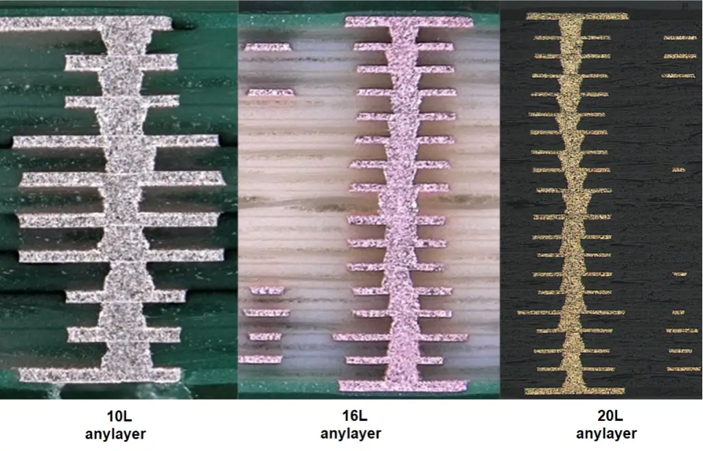
Anylayer HDI PCB (Any Layer HDI)
Our anylayer HDI PCB—also referred to as any layer HDI technology—is a high-end offering that enables direct connections between any two layers via laser-drilled microvias. This eliminates the need for buried vias in most scenarios, pushing component density 50% higher than traditional HDI alternatives. With tight impedance control of ±3%, this technology is tailored for high-frequency applications such as radar systems and satellite communication equipment.
HDI Rigid Flex PCB Solutions
Our HDI rigid-flex PCBs integrate high-density interconnect technology with flexible circuit substrates, merging the structural stability of rigid HDI boards with the bendable versatility of flexible PCBs. Microvias are seamlessly incorporated into both rigid and flexible sections, and the boards achieve a minimum bending radius of 0.5 times the board thickness. This makes them ideal for use in automotive ADAS sensors and implantable medical devices where space and flexibility are critical.
HDI PCB Manufacturing Process
HDI PCB Fabrication Workflow
Our HDI PCB production process adheres to rigorous IPC standards and consists of 5 core stages:
- High-precision laser drilling to create microvias and staggered microvias with pinpoint accuracy;
- Plasma desmear treatment to remove resin residue and ensure reliable via conductivity;
- Sequential lamination for assembling complex multilayer HDI PCB structures;
- Electroless Nickel Immersion Gold (ENIG) surface finishing to optimize solderability and corrosion resistance;
- 100% X-ray inspection to verify via quality and detect potential defects before shipment.
Our production lines cater to both prototype orders (1–100 units) and large-scale mass production (100,000+ units), with lead times ranging from 7 to 15 days.
HDI Board Design Guidelines
Our HDI design engineering team offers free Design for Manufacturing (DFM) consulting services for all HDI PCB projects. Key design guidelines we recommend include:
- Maintain a minimum microvia diameter of 0.1mm to ensure manufacturability and reduce production costs;
- Adopt staggered microvias for high-density PCB designs to maximize space utilization;
- Reserve a minimum spacing of 0.2mm between microvias and surface-mounted components to prevent soldering issues.
We also provide standardized HDI board design templates, which can cut design revision cycles by up to 30%.
Why Choose Our HDI PCB Services
Certified HDI PCB Manufacturer
As a professional HDI PCB manufacturer and supplier, we hold a suite of industry-leading certifications, including IPC-A-600, IPC-610, and ISO 13485 (for medical device applications). Our production facilities are also compliant with IATF 16949 automotive industry standards. We maintain full traceability across the entire production chain, from raw material procurement (Rogers/FR-4 substrates) to final product delivery. Our engineering team boasts over 10 years of specialized experience in HDI technology, focusing on high-reliability sectors such as aerospace, medical, and automotive.
HDI PCB Cost & Quotation Factors
The cost of HDI PCBs is determined by four primary factors:
- Layer count: Anylayer HDI PCBs are typically 30–50% more costly than 2N2 HDI alternatives due to their complex manufacturing process;
- Microvia type: Staggered microvias add 15–20% to the overall cost compared to standard microvias, owing to their precision alignment requirements;
- Base material: Rogers high-frequency materials double the cost relative to standard FR-4 substrates, reflecting their superior performance in high-speed applications;
- Order volume: Prototype orders range from $50 to $200 per square inch, while mass production volumes drive costs down to $5–$15 per square inch.
We commit to transparent, all-inclusive quoting with no hidden fees for all HDI PCB projects.
HDI PCB Application Cases
5G Telecom HDI PCB Case
We partnered with a leading 5G base station manufacturer to deliver custom anylayer HDI PCBs, incorporating staggered microvias and Rogers 4350B high-frequency material to achieve ±3% impedance control. The resulting multilayer HDI PCBs reduced the base station module size by 40% and enhanced signal integrity across the 24–40GHz frequency band. We successfully delivered over 100,000 units with zero quality defects, meeting the client’s strict deployment timelines.
Medical Device HDI Rigid Flex PCB Case
Our HDI rigid-flex PCBs were integrated into a portable diagnostic device, with flexible sections enabling seamless bending and rigid sections providing a stable platform for component mounting. The microvia design optimized power efficiency, achieving a standby power consumption of ≤10mW. The product fully complied with FDA 21 CFR Part 820 regulations, helping our client accelerate time-to-market by 2 months.
HDI Multilayer PCB Capabilities
An HDI board requires smaller vias to make layer transitions, particularly in fine-pitch BGA components and more traces per sq. mm. In order to accommodate fine-pitch components, you’ll find the following typical features in an HDI layout:
Smaller vias: HDI boards use microvias (mechanically or laser drilled), blind/buried, and staggered vias for layer transitions. These vias have smaller aspect ratios than typical through-hole vias. In order to use these vias with finer pitch components, their diameters are smaller, which then limits their useful depth.
Thinner traces: The thinner traces used in HDI boards are required to make connections to vias on each layer, as well as to in-pad vias. The thinner traces also allow higher trace density, thus the term HDI.
Higher layer count: We’ve built non-HDI boards with high layer counts, but HDI board layer counts can easily reach 20 or more layers when working with high pin density components (e.g., FPGAs).
Lower signal levels: HDI boards are not used for high voltage or high current. This is because the high field strength between neighboring lines will cause ESD, and high currents will cause excessive temperature rise in conductors.
HDI PCB Design Guidelines
Download our design guidelines for HDI PCBs
To prevent getting it wrong from the start, we have put together our design guidelines, to use as a checklist.
The file lists some of the fabrication features that are typically associated with HDI. The feature limits listed are not comprehensive; Our experienced engineers have also worked with every type of PCB material, so they have the knowledge and expertise to provide recommendations and answer all of your HDI PCB questions. Most importantly, they know how to assist for manufacturability and the potential cost drivers of a project.
| Description | Production | Advanced |
|---|---|---|
| Structure | 3+n+3 (8+N+8 MAX) | 9+N+9 |
| Layer Count | 2~80L | 100L |
| Min. Board thickness | 0.005" (+/-10%) | 0.005" (+/-10%) |
| Max. Board thickness | 0.300" (+/-10%) | 0.350" (+/-8%) |
| BGA Pitch | 8mils (0.2mm) | 6mils (0.15mm) |
| Min.BGA pad/space | 7mils/3mils | 5mils/2mils |
| Materials for build up | ||
| Prepreg (FR4 1067/1086/2113) | Yes | Yes |
| Prepreg (ceramics Ro4350) | Yes | Yes |
| Laser Drillable Prepreg | Yes | Yes |
| laser Drillable core (FR4, PI, PTFE, ceramics) | Yes | Yes |
| laser Drillable Min.Dielectric thickness | 2mils | 1.5mils |
| laser Drillable Max.Dielectric thickness | 4mils | 5mils |
| Laser via | ||
| Min / Max | 2.5mils / 6mils | 2mils / 6mils |
| Min via edge to via dege space | 6mils | 5mils |
| True position Tolerance | +/-1mils | +/-1mils |
| Drilling | ||
| Min. Drilled blind via diameter (as drilled) | 6mils | 5mils |
| Min via edge to via dege space (as drilled) | 8mils | 7mils |
| PTH Design | ||
| Blind via aspect ratio (dielectric thickness/ Laser drill hole size) | 0.8 | 1 |
| Blind via plating thickness | 0.3~1mils | 0.3~1mils |
| Capture pad A/R | 2.5mils | 2mils |
| Laser via Fill Material | Epoxy resin/Copper paste | Epoxy resin/Copper paste |
| Blind via aspect ratio (as drilled) (dielectric thickness/ drilling hole size) | 0.5 | 0.5 |
| Blind via plating thickness (as drilled) | 0.8mils | 1.0mils |
| Capture pad A/R (as drilled) | 3mils | 2mils |
| Outer Layer | ||
| Min. Trace/Space | 2mils / 2mils | 1.5mils / 1.5mils |
| Min. pad over drill size | 6mils | 5mils |
| Max. Copper thickness | 12 oz | 30 oz |
| Line/ pad to board edge | 8mils | 7mils |
| Line Tolerance | +/-15% | +/-10% |
| Inner Layer | ||
| Min.Trace/Space | 1.5mils / 1.5mils | 1.2mils / 1.5mils |
| Min. Copper Thickness | 1/3oz | 1/7 oz |
| Max. Copper Thickness | 10oz | 12oz |
| Min. Core Thickness | 2mils | 1.5mils |
| Line/ pad to drill hole | 7mils | 6mils |
| Line/ pad to board edge | 8mils | 7mils |
| Line Tolerance | +/-10% | +/-10% |
View More +
HDI PCB 1 n 1
This is the simplest HDI PCB design structure suitable for BGA with lower I/O counts. It has a fine line, microvias and registration technologies capable of 0.4 mm ball pitch, excellent mounting stability and reliability, and may contain copper filled via.
In this 1-N-1 type of stack-up, the ‘1’ represents one sequential lamination on either side of the core. One sequential lamination adds two copper layers for a total of N+2 layers. This stack-up does not feature stacked vias. There is one extra lamination and no stacking of the vias. The buried via has been mechanically-drilled. There is no need to use a conductive fill for the via. It will naturally fill with the dielectric material. The second lamination adds the top and bottom layers. Then, we finish up with a final mechanical drill. The pcb manufacturer plans the right amount of prepreg between layer one and two so the resin flows into the buried via.
HDI PCB 2 n 2
2+N+2 in PCB manufacturing refers to a stack-up structure in the design of a printed circuit board. The numbers 2 and 2 represent the number of copper layers (or other materials) in the core of the board, which provides the electrical connection and stability for the components. The “N” refers to the number of additional signal layers that can be added between the core layer. The value of “N” is determined by the complexity and number of electrical connections needed on the PCB.
For example, the term “4+n+4” in the sequential lamination of printed circuit boards refers to the number of layers used in the manufacturing process of a PCB.
The stack-up structure is crucial in determining the overall electrical performance, signal integrity, and thermal management of the PCB. By having 4 layers in the core and additional N layers in the inner portion, the designer can optimize the routing, shielding, and decoupling strategies to meet the electrical requirements of the board. The additional 4 layers in the core provide additional stability and improve the mechanical integrity of the board.
Overall, the 4+N+4 stack-up structure in PCB manufacturing provides a balanced design that offers the necessary electrical performance, reliability, and mechanical strength for the printed circuit board.
Anylayer pcb
These are PCBs that enable free connection between all layers combining laser technology and filled plating technology that allows ultra-fine processing. With the higher degree of design freedom and higher-density wiring, these PCBs are ideal for the needs of downsizing and thinning of smartphones and other high performance devices.
Any layer hdi pcb is sometimes referred to as any-layer HDI, meaning signals can be routed on high density interconnects between any layer in the stackup. These advanced HDI PCBs contain multiple layers of copper-filled stacked in-pad microvias that enable even more complex interconnections. When using any layer hdi pcb on an HDI board, each layer has its own copper-filled, laser-drilled microvias. any layer hdi pcb uses only stacked copper-filled microvias to make connections through each layer. This allows connections to be made between any two layers in the PCB once the layers are stacked. Not only does this offer an increased level of flexibility, but it also allows designers to maximize interconnect density on any layer.
HDI Printed Circuit Board Structure
The Institute for Printed Circuits (IPC-2226) provides six design structures for HDI printed circuit boards. These designs are defined by the IPC-2226 standard. Every structure can be represented by the notation i+[C]+i, with i indicating the number of layers on each side of the “core”: which is represented as [C]. The core of a PCB is the rigid base material onto which copper traces are imprinted. Below are the three most commonly used structures in the manufacture of HDI printed circuit boards.
In the IPC-2226 specification, HDI features are classified into three types:
- Type I: Microvia features, with a size of 0.15 mm (6 mils) or less.
- Type II: Blind via features, where the via does not pass through the entire board and terminates on an internal layer. The size of Type II vias is typically between 0.15 mm and 0.50 mm (6 mils to 20 mils).
- Type III: Through-hole via features, where the via passes through the entire board and extends out through both sides. The size of Type III vias is typically greater than 0.50 mm (20 mils).
Each type of HDI feature is designed to meet specific requirements and is used in different applications. The IPC-2226 specification provides design guidelines and performance criteria for HDI features and is widely used in the electronics industry as a reference for the design and manufacture of high-density printed circuit boards.
Based on the IPC-2315 standard from the Institute of Printed Circuits (IPC), fabricators may use HDI PCB stackup of types I, II, III, IV, V, or Vi. Of the above, types IV, V, and VI are more expensive to fabricate and usually not suitable for high density PCBs with challenges of routing and BGA breakout.
Manufacturability of HDI design primarily has to do with via structures. Microvia structures can have a big impact on the manufacturing process since they directly affect the number of lamination cycles. The more variations you have of layers where microvias start and stop at, the more number of sequential laminations are needed for the PCB manufacturing.
Any Layer HDI PCB Fabrication
The any layer hdi pcb manufacturing process starts with an ultra-thin core with laser-drilled microvias and a solid copper-filled base. After the initial microvia on an inner layer is filled with copper, the next dielectric layer is added in sequential lamination. Laser drilling is applied to the new layer to build the any layer hdi pcb PCB stacked, followed by filling the vias in that layer with copper. This is repeated until the desired stack is built with copper-filled microvias. The sequential copper fill improves the structural integrity of the board and is needed to prevent dimpling/voiding in the interior microvias as long as buildup produces strong plating interfaces should stacked microvias be used.
Sequential Lamination Cycles
Sequential lamination of PCBs is a process where multiple layers of metal and insulating materials are stacked and laminated together in a sequential manner. This process is used to build multi-layer PCBs that have more complex and dense circuit layouts. In sequential lamination, each layer is added one by one, with a dry film photoresist material being applied on top of each layer and then etched to form the desired pattern. This process is repeated for each layer, and after all the layers are assembled, the entire stack is pressed and cured under heat and pressure to form a solid and highly dense PCB.
Each lamination cycle or a sequential lamination process involves stacking the desired number of layers of material, followed by the application of heat and pressure to bond the layers together. The process is repeated for each cycle until the desired final thickness is achieved.
Challenges Faced in Sequential Lamination Cycles In Printed Circuit Boards
- Lamination Consistency: Ensuring consistent lamination quality across multiple cycles is a major challenge, as it is difficult to control the uniformity of pressure, temperature, and time, leading to uneven lamination.
- Delamination: Delamination is a common issue that occurs when the bond between the layers of a printed circuit board weakens or fails. This can occur due to multiple lamination cycles, which increase the risk of delamination and can result in the circuit board failing.
- Warping: Warping is another common problem associated with multiple lamination cycles. Warping occurs when the printed circuit board is not evenly heated and cooled, leading to distortion of the circuit board and causing it to become warped.
- Lamination Defects: Lamination defects, such as air bubbles, cracks, and voids, can occur during the lamination process. These defects can weaken the circuit board and reduce its reliability.
- Material Compression: Multiple lamination cycles can also result in material compression, which can cause the printed circuit board to lose its original thickness. This can impact the performance and reliability of the board.
HDI Circuit Board Application
Moblie:
Smart Phone/Tablet
In line with the trend of high functionality of mobile devices, our company is applying Build up Stack-via, Staggered via, Filled via & Fine Pitch to the manufacturing process for small/high density, high quality PCB.
Memory Module(DIMM/SODIMM): DeskTop PC / Notebook PC / Workstation / Server
To improve the performance of PCs that require speedy processing of large sized of data, our company provides PCBs for DIMMs and SODIMMs in various forms, and also provides Customization options for servers or workstations.
SSD:
DeskTop PC/Notebook PC/Workstation/Server
With its low power consumption and high processing speed, the SSD (solid state drive) is emerging as a prospective environment friendly storage device for the next generation. It will eventually become the standard sub storage device for PCs. Currently, our company is providing multi layered, high quality PCB.
Display(LCD/OLED):
OLED TV / PCMointor / NoteBook Monitor / Mobile, Tablet Display
Display is expected to continue to grow along with the rapid development of the information and communication industry. Recently, high resolution, high integration, thin thickness and light weight are required. In addition, Our Company is providing Build up Stack via, Staggered via, Filled via and fine pitches are according to customer needs to provide high-density, high-quality PCB applicable to various display products.
Get started with HDI PCB
- Blind vias, buried vias, Ultra HDI PCB
- High frequency low loss PCB material
- Low loss high speed PCB materials
- R-5775, R-5785, R-5795, TU-872 SLK , TU-872 SLK SP, TU 933+, I-Tera MT40, Astra MT77, Tachyon 100G material
- EM-888, EM-888(S), EM-888(K), EM-526, EM-528, EM-528K, IT-968, IT-968 SE, IT-988G, IT-988G SE material