
HDI PCB Impedance Control: Complete Engineering Reference
Electronic engineers designing high density interconnect PCBs and procurement teams sourcing them face persistent challenges balancing signal integrity, miniaturization, and manufacturing consistency. Uncontrolled impedance in HDI circuit boards causes signal reflections, crosstalk, and data errors—especially critical for high-speed applications like AI servers, 5G modules, and medical devices. Procurement teams also struggle to align supplier capabilities with impedance tolerance requirements, leading to costly reworks or failed production runs. HDI PCB impedance control, the practice of maintaining precise electrical impedance across micro-traces and interconnects, solves these pain points. This guide delivers factory-engineer insights, actionable parameters, and real-world manufacturing expertise to master impedance control for high density interconnect PCBs.
Learn more about: Signal Integrity in HDI PCB Design
What Is PCB Impedance Control?
Core Definition & IPC Classification
PCB impedance control is the precision design and fabrication practice of maintaining consistent electrical impedance—measured in ohms (Ω)—across signal transmission lines. It balances resistance, capacitance, and inductance to ensure signals travel without reflection or distortion. Per IPC-2221 (generic PCB design standards) and IPC-6016 (HDI-specific performance specs), impedance control is mandatory for high-speed HDI PCBs operating at ≥1Gbps. For high density interconnect PCBs, this practice is amplified due to finer trace widths, tighter spacing, and complex stackups, making consistent impedance critical for preserving signal integrity in compact form factors.
Unique Characteristics in HDI PCBs
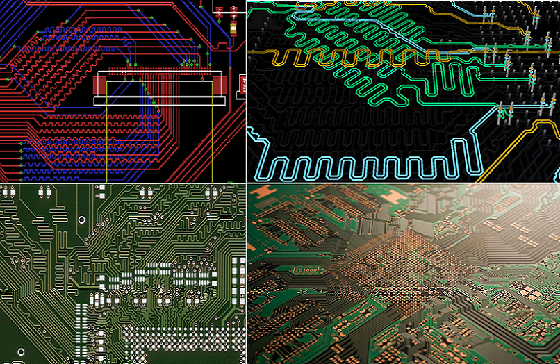
HDI PCB impedance control differs from standard PCB practices due to the structural demands of high density interconnect designs:
- Micro-traces (20–50μm width) are far more sensitive to dimensional variation
- Multi-layer build-up structures (1+N+1, 2+N+2) require uniform dielectric thickness
- Microvias (25–150μm) create localized impedance discontinuities that require compensation
- Fine-pitch components (0.2–0.5mm BGAs) demand impedance matching at the pad-via interface
- Higher routing density increases crosstalk risk, making controlled impedance a primary mitigation method
Purpose & Benefits of HDI PCB Impedance Control
Functional Objectives for High-Speed Reliability
Impedance control fulfills four critical roles in high density interconnect PCBs:
- Eliminate Signal Reflections: Reduces reflection coefficients to ≤0.1 for signals up to 50Gbps
- Minimize Crosstalk: Lowers near-end crosstalk (NEXT) to ≤-35dB at 25Gbps
- Stabilize Signal Propagation: Ensures consistent transmission speed across the entire board
- Maintain System Compatibility: Matches impedance between ICs, connectors, and transmission lines
Practical Value for Engineers & Procurement
From a user perspective, controlled impedance delivers measurable advantages:
- Reduces field failure rates by up to 30% in high-speed applications
- Lowers prototype iteration costs by approximately 25%
- Enables 30–40% smaller board footprints without performance loss
- Improves volume production yield to 92–96%
- Simplifies supplier qualification with clear, IPC-aligned standards
Critical Controlled Impedance Values
Standard Impedance Specifications
Industry-standard impedance values for high density interconnect PCBs are application-specific:
| Application | Impedance Type | Target Value | Tolerance (Practical/IPC-6016) |
|---|---|---|---|
| High-Speed Digital | Single-Ended | 50Ω | ±3% (High-Speed), ±5% (Standard), ±7% (Custom) |
| Ethernet / PCIe | Differential | 100Ω | ±3% (High-Speed), ±5% (Standard), ±7% (Custom) |
| USB 3.2 / HDMI | Differential | 90Ω | ±5% (Standard), ±7% (Custom) |
| Video / RF | Single-Ended | 75Ω | ±5% (Standard), ±7% (Custom) |
| Automotive CAN | Differential | 120Ω | ±10% (Standard), ±7% (High-Reliability Custom) |
Tolerance Classes for HDI Production
- Class 3 (medical/aerospace): ±3% tolerance, high-precision processes required
- Class 2 (industrial/consumer): ±5% tolerance, standard for most HDI production
- Class 1 (non-critical): ±10% tolerance, rarely used in high-speed designs
- Microvias cause a 2–4% impedance drop, requiring trace width compensation
Factors That Determine Impedance in HDI PCBs
Primary Design & Material Drivers
Impedance in HDI PCBs is determined by five measurable parameters:
- Trace geometry: 20–50μm width, 12–35μm copper thickness
- Dielectric constant (Dk): 3.0–4.5 for standard and high-performance materials
- Dielectric thickness: 10–50μm for build-up layers, 100–400μm for core layers
- Reference plane distance: Directly proportional to impedance level
- Microvia properties: Diameter, plating, and depth affect local impedance
Environmental & Process Influences
Real-world conditions create measurable impedance shifts:
- Temperature: 0.02–0.1Ω per °C depending on material
- Humidity: Up to 3Ω increase at high relative humidity
- Etching variation: ±2μm width = ±1Ω impedance change
- Lamination pressure: Alters dielectric thickness and final impedance
Design & Manufacturing Requirements
HDI PCB Design Rules for Impedance Stability
Engineers must follow numerical design rules for consistent impedance:
- Trace width calculated for target impedance, dielectric, and copper weight
- Differential pair spacing set to 1.5–2x trace width
- No reference plane splits under controlled-impedance traces
- Microvia placement ≥50μm from trace edges with width compensation
- Symmetric stackups preferred to avoid layer-to-layer variation
Manufacturing Process Controls
HDI PCB factories use specialized processes to maintain precision:
- Laser etching: ±2μm trace width accuracy
- Pressure-controlled lamination: ±3μm dielectric thickness control
- Uniform copper plating: ±1μm thickness variation
- Planarization: ≤5μm surface flatness
- Low-CTE materials to reduce thermal drift
- TDR test coupons on every production panel
Core Impedance Specifications for HDI PCBs
Single-Ended vs. Differential Impedance
- Single-ended: 20–50μm traces, single reference plane, used for control and RF signals
- Differential: 25–45μm traces per line, length-matched to ±50μm, used for high-speed data
HDI-Specific Adjustments
- Microvia compensation: 5–10% wider traces near vias
- Build-up layer influence: each layer adds 1–2Ω to differential impedance
- BGA escape routing: limited neck-down with impedance compensation
- Rigid-flex designs: adjusted trace width for flex dielectric regions
Design Factors Shaping HDI Impedance
Stackup & Layer Configuration
Stackup design directly defines impedance behavior:
- 1+N+1: Microstrip outer layers, stripline inner layers
- 2+N+2: Symmetric build-up layers for balanced impedance
- Asymmetric stackups can cause ±5% impedance mismatch
Trace Routing & Component Integration
Routing discipline prevents impedance discontinuities:
- Bend radius ≥3x trace width
- Gradual tapering for neck-down sections
- Pad size limited to ≤2x trace width
- Back-drilling for via stubs over 50μm
Manufacturing Requirements for Precision Control
Process & Equipment Capability
Stable impedance requires advanced manufacturing equipment:
- UV laser etching with ±1μm accuracy
- Precision lamination presses with tight temperature and pressure control
- Pulse plating for uniform copper distribution
- High-resolution TDR testers (0.1Ω resolution)
- 3D X-ray and AOI for dimensional verification
Quality Control & Verification
Full impedance compliance requires multi-stage inspection:
- In-process trace width and dielectric measurement
- 100% TDR testing on coupons per IPC-2221
- Impedance mapping for Class 3 boards
- Cross-section analysis for process validation
Performance Benefits for HDI PCB Applications
Measurable Technical Improvements
| Metric | Without Impedance Control | With Precision Control | Improvement |
|---|---|---|---|
| Signal Speed | ≤10Gbps | Up to 50Gbps | 5x |
| Crosstalk (NEXT) | ≤-20dB | ≤-35dB | 15dB |
| Bit Error Rate | 10⁻⁶ | 10⁻¹² | 6 orders |
| Thermal Stability | ±10Ω | ±2Ω | 80% |
| Routing Density | 80 pins/in² | 120+ pins/in² | 50% |
Application-Specific Value
Impedance control enables performance in key markets:
- AI & data centers: 25–50Gbps signal integrity
- 5G infrastructure: reduced loss and extended range
- Medical devices: long-term stability and accuracy
- Automotive: reliability across extreme temperatures
- Consumer electronics: miniaturization without performance loss
High-Speed HDI PCB Impedance
Design Rules for 25Gbps+ Signals
- Narrow, thin traces to reduce skin effect
- Low-loss dielectrics (Df ≤0.005)
- Tight ±2% impedance tolerance
- Back-drilled vias to eliminate stubs
- Increased spacing to control crosstalk
High-Speed Challenges & Solutions
- Dispersion: mitigated with low-Dk materials
- Thermal drift: stabilized by low-CTE laminates
- Manufacturing variation: controlled with SPC limits
- Discontinuities: resolved with tapered trace transitions
Low-Loss Materials for HDI Impedance Control
Material Selection Comparison
| Material Type | Dk | Df | TCEr | Max Speed |
|---|---|---|---|---|
| Standard FR-4 | 4.2–4.6 | 0.015–0.020 | 100–200 | ≤10Gbps |
| High-Tg FR-4 | 4.0–4.3 | 0.012–0.015 | 80–150 | ≤25Gbps |
| Low-Loss FR-4 | 3.8–4.0 | 0.008–0.010 | 50–100 | ≤40Gbps |
| Ceramic-Filled | 3.0–3.5 | 0.003–0.005 | 30–60 | ≤45Gbps |
| PTFE-Based | 2.1–2.3 | 0.001–0.002 | 20–50 | ≤50Gbps |
Material Impact on Impedance Stability
- Dk stability over frequency reduces drift by 70%
- Low moisture absorption limits humidity-related shift
- High thermal conductivity reduces temperature-induced error
- CTE matching minimizes stress-related impedance change
Learn more about :PCB Material
Real Factory HDI PCB Impedance Control Case Study
Project Overview
An 8-layer 2+4+2 high density interconnect PCB for a 5G communication module:
- Impedance: 50Ω SE (±3%), 100Ω diff (±3%)
- Trace/space: 25μm/25μm
- Board thickness: 0.8mm
- Low-loss FR-4, 25Gbps signals
- Target yield: ≥93%
Initial Challenges
Pilot production yielded only 76% due to:
- Trace width variation causing impedance shift
- Inconsistent build-up dielectric thickness
- Uncompensated microvia impedance drop
Solutions & Results
- Laser etching calibrated to ±2μm
- Lamination pressure optimized for uniform dielectric
- 8% trace width compensation near microvias
Final results:
- Yield improved to 95%
- Impedance held within ±2Ω for single-ended, ±3Ω for differential
- 0.4% rework rate, zero field failures
Common Design Errors (Production End Perspective)
Impedance-Specific Mistakes
From factory engineering view, 85% of failures come from:
- Missing microvia impedance compensation
- Abrupt trace neck-down beyond 20%
- Reference plane splits under critical traces
- Incorrect Dk values used in simulation
- Poor differential pair length or spacing control
Stackup & Manufacturing Misalignment
- Unrealistically tight impedance tolerances
- Dielectric thickness below factory capability
- Overly heavy copper for fine traces
- Missing impedance test coupons
FAQ – HDI PCB Impedance Control
1. Single-ended vs. differential impedance: which to use?
Use single-ended (50Ω) for control signals, RF, and low-speed data. Use differential (90/100/120Ω) for high-speed signals ≥10Gbps, as they provide superior noise immunity and crosstalk resistance.
2. What is the minimum trace width for impedance-controlled HDI PCBs?
The volume-production minimum is 20μm for 50Ω impedance. For Class 3 applications, 25μm is recommended for stability and yield.
3. How do microvias affect HDI impedance?
Microvias cause a 2–4Ω impedance drop due to increased local capacitance. Compensate with 5–10% wider traces within 500μm of the via.
4. Best material for stable impedance in harsh environments?
Ceramic-filled low-loss laminates provide the best balance of stability, temperature resistance, and cost. For RF, PTFE-based materials offer the lowest loss and highest stability.
If you need HDI PCB with impedance control,contact our engineering team for a free DFM check.


![Understanding PCB Costs & Pricing [Your Complete Guide]](https://hdicircuitboard.com/wp-content/uploads/elementor/thumbs/Understanding-PCB-Costs-Pricing-Your-Complete-Guide-qzzhe6mcaxuolkux3xalfktgavumi9y1aqfbs9bpv4.webp "Understanding PCB Costs & Pricing [Your Complete Guide]")


