
HDI PCB Stack Design: 1+N+1 to 4+N+4 Complete Guide
Electronic engineers designing high density interconnect PCBs and procurement teams sourcing them face persistent challenges balancing routing density, signal integrity, and manufacturing feasibility. Many struggle to select the right HDI stackup structure—1+N+1, 2+N+2, 3+N+3, or 4+N+4—for their specific application, while procurement teams often grapple with cost variations and lead time differences across stackup types. Choosing the wrong HDI stackup leads to reworks, signal degradation, or over-engineered solutions that drive up costs. This guide breaks down each core HDI stackup structure from a factory engineer’s perspective, with actionable parameters, real production insights, and clear selection frameworks to master high density interconnect PCB stack design.
Learn more about : What’s HDI? Design Basics and Complete HDI PCB Manufacturing Process
What is PCB Stackup?
Core Definition & HDI-Specific Purpose
PCB stackup is the layered arrangement of copper conductors, dielectric materials, and prepregs that forms the foundation of a printed circuit board. For high density interconnect PCBs, stackup design is elevated to a precision engineering practice—dictating routing density, signal integrity, and manufacturing complexity—by integrating sequential build-up (SBU) layers and specialized via structures. Per IPC-2221 (generic PCB design) and IPC-6016 (HDI-specific performance), HDI stackups must support microvias (≤150μm diameter), blind/buried vias, and fine line/space geometries (≥20μm) while maintaining structural stability.
Distinction in HDI PCB Context
HDI PCB stackups differ fundamentally from conventional PCB stackups due to their focus on miniaturization and high-speed performance:
- Sequential build-up layers (added to core sides) enable microvia integration
- Symmetrical layer arrangement to prevent warpage (critical for thin HDI boards)
- Tight dielectric thickness control (±3μm) for impedance consistency
- Dedicated power/ground plane pairs to reduce crosstalk (≤-35dB at 25Gbps)
- Compatibility with via-in-pad and stacked microvia technologies
Common HDI Stackup Structures
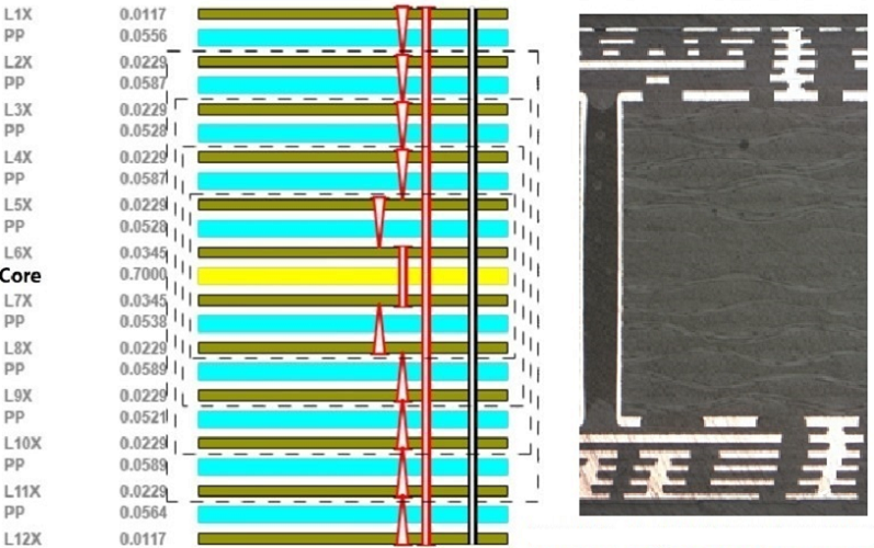
i+N+i Nomenclature Explained
All core HDI stackup structures follow the i+N+i notation, a universal language for communicating build-up complexity to manufacturers:
- i: Number of sequential build-up layers added to each side of the central core
- N: Number of layers in the rigid central core (may include buried vias)
- Example: 2+8+2 = 2 build-up layers per side + 8-layer core = 12 total layers
- Build-up layers: 10–30μm dielectric thickness (resin-coated copper, RCC)
- Core layers: 100–400μm dielectric thickness (FR-4, high-Tg, or low-loss materials)
Key Structural Comparison
| HDI Stackup Type | Total Layers (Typical) | Build-Up Layers (Per Side) | Core Layers (N) | IPC-2226 Equivalent |
|---|---|---|---|---|
| 1+N+1 | 4–10 | 1 | 2–8 | Type I/II |
| 2+N+2 | 8–16 | 2 | 4–12 | Type III |
| 3+N+3 | 14–22 | 3 | 8–16 | Type III (Advanced) |
| 4+N+4 | 18–28 | 4 | 10–20 | Type IV–VI |
Learn more about: Cost Differences Between 1+N+1, 2+N+2, and Any-Layer High Density Interconnect (HDI) PCBs
1+N+1 HDI Stackup
Structural Details & Parameters
The 1+N+1 HDI stackup is the entry-level high density interconnect structure, ideal for cost-sensitive designs requiring moderate density:
- Layer Composition: 1 build-up layer (RCC, 10–20μm dielectric) on top/bottom of N-layer core
- Via Compatibility: Laser-drilled microvias (50–100μm diameter) connecting build-up layers to core
- Line/Space: 25–50μm (outer layers), 30–60μm (core layers)
- Copper Weight: 0.5oz (18μm) build-up layers, 0.5–1oz (18–35μm) core layers
- Finished Thickness: 0.4–1.6mm (4-layer: 0.4–0.8mm; 10-layer: 1.2–1.6mm)
- Impedance Control: ±5–10% tolerance (50Ω single-ended, 100Ω differential)
Manufacturing & Application Traits
- Lamination Cycles: 1 press cycle (simplest HDI manufacturing)
- Lead Time: 5–10 days (quick turn capability for prototypes)
- Yield Rate: 95–98% (lowest complexity, fewest failure points)
- Ideal Applications: Basic smartphones, wearables, low-cost consumer electronics, industrial sensors
- Cost Position: 30–40% lower than 2+N+2 for equivalent layer count
2+N+2 HDI Stackup
Structural Details & Parameters
The 2+N+2 HDI stackup is the most balanced high density interconnect structure, striking a sweet spot between performance and cost:
- Layer Composition: 2 sequential build-up layers (10–20μm dielectric each) on top/bottom of N-layer core
- Via Compatibility: Stacked/staggered microvias (50–100μm), blind vias (100–150μm), buried vias (core)
- Line/Space: 20–40μm (outer build-up), 25–50μm (inner build-up/core)
- Copper Weight: 0.5oz (18μm) build-up layers, 0.5–2oz (18–70μm) core layers
- Finished Thickness: 0.8–2.0mm (8-layer: 0.8–1.2mm; 16-layer: 1.6–2.0mm)
- Impedance Control: ±3–5% tolerance (supports up to 50Gbps signals)
Manufacturing & Application Traits
- Lamination Cycles: 2 press cycles (sequential build-up of outer layers)
- Lead Time: 7–14 days (prototypes), 15–25 days (volume production)
- Yield Rate: 92–95% (higher complexity than 1+N+1)
- Ideal Applications: Flagship smartphones, laptops, 5G modules, automotive ADAS, high-speed routers
- Cost Position: Benchmark for high-performance HDI PCBs; 15–20% premium over 1+N+1
3+N+3 HDI Stackup
Structural Details & Parameters
The 3+N+3 HDI stackup is an advanced high density interconnect structure for complex, high-pin-count designs:
- Layer Composition: 3 sequential build-up layers (10–15μm dielectric each) on top/bottom of N-layer core
- Via Compatibility: Fully stacked microvias (50–80μm), blind/buried vias, via-in-pad (copper-filled)
- Line/Space: 15–35μm (outer build-up), 20–40μm (inner build-up/core)
- Copper Weight: 0.5oz (18μm) build-up layers, 1–2oz (35–70μm) core layers
- Finished Thickness: 1.2–2.5mm (14-layer: 1.2–1.6mm; 22-layer: 2.0–2.5mm)
- Impedance Control: ±2–3% tolerance (supports up to 60Gbps signals)
Manufacturing & Application Traits
- Lamination Cycles: 3 press cycles (precision alignment required)
- Lead Time: 10–18 days (prototypes), 20–30 days (volume production)
- Yield Rate: 88–92% (requires advanced manufacturing capabilities)
- Ideal Applications: High-performance computing (HPC), AI accelerators, aerospace electronics, complex SoCs
- Cost Position: 40–60% premium over 2+N+2; requires specialized fabrication
4+N+4 HDI Stackup
Structural Details & Parameters
The 4+N+4 HDI stackup is the most complex high density interconnect structure, reserved for extreme performance requirements:
- Layer Composition: 4 sequential build-up layers (10–15μm dielectric each) on top/bottom of N-layer core
- Via Compatibility: Ultra-fine microvias (40–80μm), fully stacked via-in-pad, blind/buried vias (all layers)
- Line/Space: 12–30μm (outer build-up), 15–35μm (inner build-up/core)
- Copper Weight: 0.5oz (18μm) build-up layers, 1–2oz (35–70μm) core layers
- Finished Thickness: 1.6–3.0mm (18-layer: 1.6–2.0mm; 28-layer: 2.5–3.0mm)
- Impedance Control: ±1–2% tolerance (supports up to 100Gbps signals)
Manufacturing & Application Traits
- Lamination Cycles: 4 press cycles (stringent alignment control)
- Lead Time: 14–25 days (prototypes), 30–45 days (volume production)
- Yield Rate: 85–90% (highest complexity, tightest tolerances)
- Ideal Applications: Cutting-edge AI modules, advanced server motherboards, satellite communication, military electronics
- Cost Position: 80–100% premium over 2+N+2; limited to high-value applications
Key Selection Factors
Design-Driven Criteria
Engineers must align HDI stackup selection with core design requirements, using numerical thresholds to guide decisions:
- BGA Pitch: ≤0.5mm pitch requires 2+N+2 or higher; ≥0.8mm pitch works with 1+N+1
- Signal Speed: ≤10Gbps: 1+N+1; 10–50Gbps: 2+N+2; 50–100Gbps: 3+N+3/4+N+4
- Routing Density: ≤80 pins/sq.in.: 1+N+1; 80–120 pins/sq.in.: 2+N+2; ≥120 pins/sq.in.: 3+N+3/4+N+4
- Layer Count Needs: ≤10 layers: 1+N+1/2+N+2; 10–20 layers: 2+N+2/3+N+3; ≥20 layers: 3+N+3/4+N+4
- Impedance Tolerance: ±5–10%: 1+N+1; ±3–5%: 2+N+2; ±1–3%: 3+N+3/4+N+4
Practical & Commercial Factors
Procurement and project teams must balance technical requirements with real-world constraints:
- Cost Target: Per-unit cost increases by 30–40% per additional build-up layer set (i)
- Lead Time: Each extra build-up layer adds 3–5 days to production time
- Manufacturer Capability: Only 15–20% of PCB factories support 3+N+3/4+N+4 stackups
- Volume Requirements: Low volume (<1k units) favors simpler stackups (1+N+1/2+N+2) to avoid NRE costs
- Supply Chain Risk: Complex stackups (3+N+3/4+N+4) have fewer qualified suppliers
Critical Stackup Design Elements
Dielectric & Copper Considerations
Core material and conductor parameters directly impact HDI stackup performance, with factory-validated ranges:
- Dielectric Materials:
- Build-up: Resin-coated copper (RCC), Dk 3.5–3.8, Df ≤0.01
- Core: High-Tg FR-4 (Tg ≥170°C) for 1+N+1/2+N+2; low-loss laminates (Dk 3.0–3.5) for 3+N+3/4+N+4
- Copper Thickness:
- Build-up layers: 0.5oz (18μm) optimal for microvia plating
- Core layers: 1oz (35μm) balances current capacity and signal integrity
- Dielectric Thickness Control:
- Build-up: ±3μm tolerance (critical for impedance)
- Core: ±10μm tolerance (structural stability)
Via & Plane Design Rules
HDI stackup performance relies on precise via and plane configuration, aligned with IPC standards:
- Microvia Aspect Ratio: ≤0.8:1 (diameter:depth) for reliable plating (IPC-6016)
- Plane Pairing: 1 power plane + 1 ground plane per 2–3 signal layers
- Plane Clearance: ≥100μm between power planes and microvia fields
- Via Staggering: Stacked vias limited to 3 layers (4+N+4) to avoid lamination voids
- Anti-Pad Sizing: 1.5x microvia diameter for plane clearance (prevents shorting)
Material Options
Dielectric Material Selection
Material choice varies by HDI stackup complexity, with tradeoffs between performance and cost:
| Material Type | Dk (10GHz) | Df (10GHz) | Tg (°C) | Stackup Suitability | Key Benefit |
|---|---|---|---|---|---|
| Standard FR-4 | 4.2–4.6 | 0.015–0.020 | 130–140 | 1+N+1 | Low cost, widely available |
| High-Tg FR-4 | 4.0–4.3 | 0.012–0.015 | 170–180 | 1+N+1/2+N+2 | Thermal stability, cost-effective |
| Low-Loss FR-4 | 3.8–4.0 | 0.008–0.010 | 160–170 | 2+N+2/3+N+3 | Balanced performance, moderate cost |
| Ceramic-Filled | 3.0–3.5 | 0.003–0.005 | 180–200 | 3+N+3/4+N+4 | Low loss, high stability |
| PTFE-Based | 2.1–2.3 | 0.001–0.002 | 260+ | 4+N+4 (RF) | Ultra-low loss, high-frequency performance |
Learn more about: How to Design HDI Microvia PCB
Copper & Filler Materials
- Copper Foil:
- Electrodeposited (ED): Standard for 1+N+1/2+N+2; low cost, moderate roughness
- Rolled Copper: Preferred for 3+N+3/4+N+4; low roughness (reduces signal loss)
- Via Fill Materials:
- Non-conductive epoxy: 1+N+1/2+N+2 (cost-effective, fast processing)
- Copper fill: 3+N+3/4+N+4 (thermal conductivity, mechanical stability)
- Prepreg:
- Standard: 1080 style for 1+N+1/2+N+2
- Fine-weave (1035/1067): 3+N+3/4+N+4 (reduces fiber weave effect)
Manufacturing Characteristics
Process Complexity & Capability Requirements
Each HDI stackup demands specific manufacturing capabilities, with clear thresholds for factory qualification:
- 1+N+1:
- Laser drilling (50–100μm), basic LDI (±2μm alignment)
- Single lamination cycle, standard plating lines
- 2+N+2:
- Sequential lamination, stacked microvia drilling
- Advanced LDI (±1μm alignment), pulse plating
- 3+N+3:
- Precision sequential lamination (±3μm layer alignment)
- UV laser drilling, copper filling, CMP planarization
- 4+N+4:
- Ultra-precision lamination (±2μm alignment)
- Multi-wavelength laser drilling, advanced inspection (3D X-ray)
Quality Control & Testing Protocols
HDI stackup quality control scales with complexity, ensuring compliance with IPC standards:
- 1+N+1:
- AOI (visual inspection), flying probe test (opens/shorts)
- Cross-section analysis (5% of production)
- 2+N+2:
- TDR impedance testing (100% of panels), X-ray inspection
- Thermal cycling (-40°C to +125°C, 100 cycles)
- 3+N+3/4+N+4:
- 3D X-ray (100% via inspection), impedance mapping
- Environmental stress testing (thermal/humidity)
- Microsection analysis (10% of production)
Performance Advantages
Signal Integrity & Electrical Performance
HDI stackup complexity directly correlates with electrical performance, with quantifiable improvements:
| Performance Metric | 1+N+1 | 2+N+2 | 3+N+3 | 4+N+4 |
|---|---|---|---|---|
| Max Signal Speed | ≤10Gbps | ≤50Gbps | ≤60Gbps | ≤100Gbps |
| Crosstalk (NEXT) | ≤-25dB | ≤-35dB | ≤-40dB | ≤-45dB |
| Impedance Stability | ±5–10% | ±3–5% | ±2–3% | ±1–2% |
| Power Delivery Efficiency | 85–90% | 90–95% | 93–97% | 95–98% |
| Routing Density (pins/sq.in.) | 60–80 | 80–120 | 120–160 | 160–200 |
Mechanical & Thermal Performance
- Mechanical Stability:
- Symmetrical stackups reduce warpage to ≤0.5% (IPC-6016 limit)
- 3+N+3/4+N+4 offer higher rigidity (critical for large-format HDI boards)
- Thermal Dissipation:
- Copper-filled vias in 3+N+3/4+N+4 improve thermal conductivity by 30–40%
- Dedicated thermal planes reduce hotspot temperatures by 15–25°C
- Reliability:
- 1+N+1: 100k thermal cycles (industrial standard)
- 2+N+2: 200k thermal cycles (consumer high-reliability)
- 3+N+3/4+N+4: 500k thermal cycles (aerospace/medical)
Factory HDI Stackup Case Study
Project Overview & Initial Parameters
A high-speed networking equipment manufacturer required an HDI PCB for a 40Gbps router module, with conflicting goals of high performance and cost efficiency:
- Key Requirements: 0.5mm pitch BGA (484 pins), 40Gbps signal support, 12-layer count, 1.6mm thickness
- Initial Stackup Choice: 1+10+1 (12-layer) – selected for cost savings
- Critical Specs: 50Ω single-ended (±5%), 100Ω differential (±5%); 25μm line/space; ENIG surface finish
Manufacturing Challenges & Root Causes
Pilot production of the 1+10+1 stackup resulted in 72% yield, failing to meet performance targets:
- Signal Integrity Failures (18% defects): 40Gbps signals suffered -20dB crosstalk (target: ≤-30dB) – root cause: insufficient build-up layers for proper grounding
- Microvia Plating Issues (7% defects): 100μm microvias had 12–15μm plating thickness (target: 18μm) – root cause: aspect ratio exceeded 1:1 in 1+10+1 structure
- Impedance Variation (3% defects): ±8% impedance drift (target: ±5%) – root cause: uneven dielectric thickness in single build-up layer
Implemented Solutions & Quantified Results
The factory recommended switching to a 2+8+2 (12-layer) stackup, with targeted process adjustments:
- Stackup Redesign: 2 build-up layers per side (15μm dielectric each) – enabled staggered microvias and additional ground plane
- Plating Optimization: Reduced microvia diameter to 80μm (aspect ratio 0.8:1) – achieved 18–20μm plating thickness
- Dielectric Control: Tightened lamination pressure to 65psi – dielectric thickness variation reduced to ±3μm
Final Results: 94% production yield, 40Gbps signal crosstalk ≤-35dB, impedance variation ±4% (meets target). Per-unit cost increased by 18% vs. 1+10+1, but total project cost decreased by 22% due to reduced rework and improved performance. The 2+8+2 stackup enabled the router module to meet latency requirements (≤10ns) and pass environmental stress testing.
Common Design Errors (Production End Perspective)
Stackup Selection Errors
From a factory engineer perspective, 70% of HDI stackup-related failures stem from incorrect structure selection:
- Over-Engineering: Specifying 3+N+3 for 10Gbps signals (1+N+1 sufficient) – increases cost by 40–60% (40% of errors)
- Under-Engineering: Using 1+N+1 for ≤0.5mm pitch BGAs – causes routing congestion and signal degradation (20% of errors)
- Ignoring Symmetry: Designing asymmetric 2+N+2 stackups – leads to warpage (≥0.8%) and assembly issues (15% of errors)
- Mismatched Via/Stackup: Using stacked vias in 1+N+1 – creates plating voids and reliability risks (10% of errors)
- Incorrect Core Layer Count: Selecting N=4 for 2+N+2 (8-layer) when N=6 is needed – reduces routing density (15% of errors)
Implementation Errors
Design implementation mistakes compound stackup issues, with avoidable manufacturing consequences:
- Inadequate Plane Pairing: <1 ground plane per 3 signal layers – increases crosstalk by 10–15dB
- Excessive Stacked Vias: >3 stacked microvias – causes lamination delamination in reflow
- Poor Dielectric Selection: Using standard FR-4 for 3+N+3 (needs low-loss material) – increases signal loss by 20–30%
- Ignoring Manufacturing Tolerances: Designing for exact dielectric thickness (no ±3μm buffer) – leads to impedance drift
- Incorrect Anti-Pad Sizing: <1.5x microvia diameter – causes short circuits between vias and planes
FAQ – HDI PCB Stack Design
1. When should I choose 2+N+2 over 1+N+1 for HDI PCBs?
Choose 2+N+2 over 1+N+1 when your high density interconnect PCB requires 0.5–0.65mm pitch BGAs, 10–50Gbps signal speeds, or 80–120 pins/sq.in. routing density. 2+N+2 is also preferred for designs needing stacked microvias or improved signal integrity (crosstalk ≤-35dB) – common in smartphones, 5G modules, and automotive ADAS. 1+N+1 remains viable for cost-sensitive, low-speed (≤10Gbps) applications with ≥0.8mm pitch components.
2. What is the maximum number of build-up layers (i) for practical HDI PCBs?
The practical maximum for most high density interconnect PCB applications is 4 build-up layers (4+N+4). While more build-up layers are technically possible, they offer diminishing returns: 5+N+5 stackups increase cost by 150–200% vs. 4+N+4 but only improve routing density by 10–15%. Additionally, <5% of PCB factories can reliably manufacture 5+N+5 stackups due to lamination alignment challenges and yield issues. 4+N+4 is reserved for extreme high-speed (≥80Gbps) or ultra-dense (≥180 pins/sq.in.) designs.
3. How does HDI stackup affect manufacturing lead time and cost?
Each additional set of build-up layers (i) increases HDI PCB manufacturing lead time by 3–5 days and cost by 30–40%. For example:
- 1+8+1 (10-layer): 7–10 days lead time, $15–20 per unit (1k volume)
- 2+8+2 (12-layer): 10–14 days lead time, $22–28 per unit (1k volume)
- 3+8+3 (14-layer): 14–18 days lead time, $35–45 per unit (1k volume)Cost drivers include additional lamination cycles, precision alignment, and advanced testing (3D X-ray, impedance mapping) required for complex stackups.
4. Can I mix build-up layer counts (e.g., 2+N+3) for HDI PCBs?
Mixing build-up layer counts (asymmetric i values) is not recommended for high density interconnect PCBs. Asymmetric stackups (e.g., 2+8+3) create uneven thermal expansion and lamination stress, leading to warpage (≥1.0% vs. ≤0.5% for symmetric) and reduced reliability. Additionally, asymmetric designs complicate impedance control (variation ±2–3% higher) and increase manufacturing complexity (custom tooling, longer setup time). IPC-2226 mandates symmetric build-up layers for HDI PCBs to ensure structural and electrical stability.


