
HDI PCB stackup design for high-speed signals provides a disciplined, manufacturing-ready approach to layer arrangement, dielectric selection, microvia configuration, and impedance control, specifically optimized for 28Gbps to 112Gbps PAM4 transmission. This guideline follows IPC‑2221, IPC‑2226, and IPC‑6016 standards, with factory-proven parameters to minimize insertion loss, crosstalk, and resonance while ensuring stable mass production yield in hdi pcb manufacturing.
Learn more about: High Speed PCB Layer Stackup: Design Guide & Examples
Key HDI Stackup Strategies for High-Speed Performance
Build-up Architecture
| Stackup Type | Max Data Rate | Dielectric | Via Type |
|---|---|---|---|
| 1+N+1 | Up to 28Gbps | 75–100 μm | Single microvia |
| 2+N+2 | 56–112Gbps | 50–75 μm | Stacked/staggered |
| Any-Layer ELIC | 224Gbps+ | 40–50 μm | Any-layer via |
Layer Arrangement
Layer sequencing follows a symmetric, noise-isolated structure to avoid warpage and ensure continuous return paths.
- High-speed differential routes placed between solid ground planes with no gaps or splits
- Power and ground planes tightly coupled (≤50 μm dielectric) for high decoupling capacitance
- Adjacent signal layers routed orthogonally to reduce crosstalk
- Overall stackup fully symmetric to control warpage ≤0.2 mm/m
- Layer registration tolerance: ±25–30 μm for reliable microvia alignment
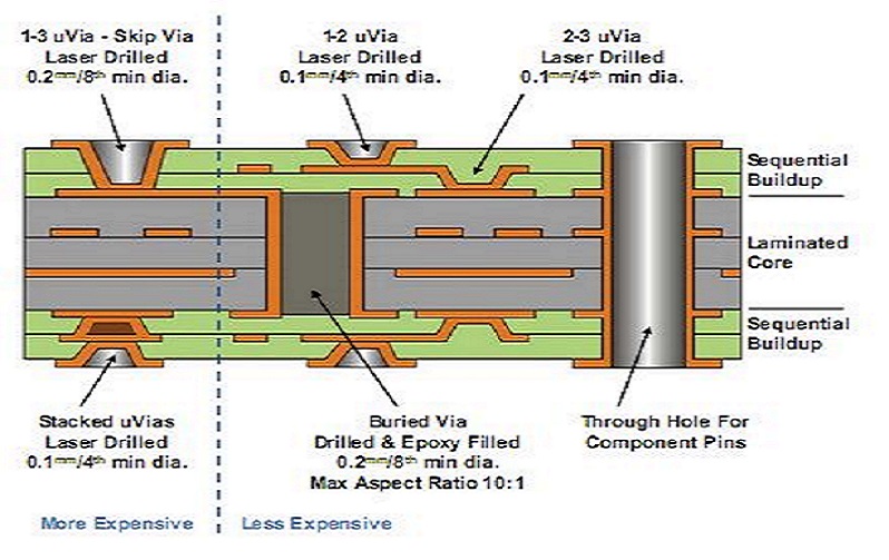
Microvias & Vias in High-Speed HDI Stackups
Microvia Specifications
Microvias are laser-drilled interconnects that replace through‑hole vias to eliminate parasitic inductance and signal resonance.
- Finished microvia diameter: 75–125 μm for high-speed channels
- Aspect ratio (depth/diameter): ≤0.75:1 (factory hard limit; >1:1 causes plating voids)
- Copper plating thickness: ≥15 μm, uniform across all microvias
- Annular ring width: ≥50 μm for structural and electrical reliability
Stacked vs Staggered Microvias
Via arrangement directly affects yield, routing density, and signal integrity in high-speed microvias pcb designs.
| Item | Stacked Microvias | Staggered Microvias |
|---|---|---|
| Space efficiency | Very high | Medium |
| Production yield | 91–94% | 96–98% |
| Filling requirement | Full copper filling | No filling required |
| Best application | Dense BGA fanout | High‑reliability 112Gbps links |
Material Selection for High-Speed HDI Stackups
Dielectric Properties
Materials are chosen for stable electrical performance at high frequencies.
- Dk: 3.3–4.0, tolerance ±0.05
- Df: ≤0.009 for 56Gbps; ≤0.007 for 800G ultra‑high‑speed designs
- Tg ≥ 170 °C to withstand lead‑free reflow at 260 °C
- Peel strength ≥0.8 kgf/cm for reliable lamination
Learn more about: High-Speed PCB Materials: A Complete Comparison Guide
Copper Foil Requirements
Low‑profile copper reduces insertion loss at 50GHz and above.
- Copper weight: 12 μm (0.5 oz) for fine signal traces; 35 μm (1 oz) for power planes
- Surface roughness Rz ≤1.5 μm for low high‑frequency loss
| Material | Df | Loss Level | Application |
|---|---|---|---|
| Standard FR-4 | 0.015–0.020 | Medium | Low-speed HDI |
| Mid-loss | 0.009–0.012 | Low | 56Gbps systems |
| Ultra-low-loss | ≤0.007 | Very low | 112G+/800G modules |
Impedance Control & Ground Referencing
Impedance Targets
Strict impedance control prevents reflection and eye closure in high-speed links.
- Single‑ended: 50Ω ±5%
- Differential: 85Ω / 100Ω ±5%
- Trace width tolerance: ±8 μm after etching
Grounding & Crosstalk Reduction
- Continuous solid ground planes under all high-speed routes
- 3W spacing rule for single‑ended signals
- Ground stitching vias at ≤1 mm pitch along guard traces
- No reference plane voids under differential pairs
Layer Thinning & Signal Integrity Techniques
Layer Thinning
Thinner dielectrics improve plane coupling and reduce parasitic effects.
- Build‑up dielectric: 40–75 μm
- Via stub length controlled to ≤20 μm to avoid resonance
Routing & Transition Rules
- Maximum 2 microvia transitions per differential pair
- Length mismatch ≤2 mm (≤5 ps skew)
- No 90° bends; use 45° or arc routing
- High-speed routes kept ≥0.5 mm from board edge
Core Technical Parameters
- Trace width/spacing: 75/75 μm – 100/100 μm
- Microvia diameter: 75–125 μm, aspect ratio ≤0.75:1
- Dielectric thickness: 40–75 μm (build‑up)
- Impedance tolerance: ±5%
- Warpage limit: ≤0.2 mm/m
- Plating thickness: ≥15 μm for microvias
Case Study
Project Details
- Stackup: 2+8+2 symmetric HDI, 12 layers
- Application: 800G optical module
- Data rate: 112Gbps PAM4
- Impedance target: 100Ω differential
Issues Found
- Insertion loss exceeded 1.1dB at 50GHz
- Crosstalk reached only −32dB (required ≤−40dB)
- Microvia aspect ratio too high, causing 7% voids
- Slight asymmetry led to 0.27 mm/m warpage
Improvements Made
- Reduced dielectric to 50 μm
- Applied ultra‑low‑loss material (Df ≤0.007)
- Optimized microvia to 0.7:1 aspect ratio
- Restructured full symmetric stackup
- Enhanced trace spacing for crosstalk control
Final Results
- Insertion loss ≤0.58dB at 50GHz
- Crosstalk improved to −46dB
- Yield increased from 78% to 95.7%
- Warpage stabilized at 0.16 mm/m
- Impedance held within ±4.1%
Common Design Errors
- Asymmetric stackup causing warpage >0.25 mm/m and impedance drift
- Microvia aspect ratio >1:1 leading to plating voids and low yield
- Reference plane gaps under high-speed traces degrading return path
- Insufficient ground stitching increasing EMI and common-mode noise
- High-roughness copper increasing insertion loss above 50GHz
Quality Control & Compliance
Testing Items
- TDR impedance measurement per IPC‑TM‑650
- Microvia cross‑section inspection for void control
- Insertion/return loss test up to 50GHz
- Thermal cycling: –40°C to 125°C, 1000 cycles
- Warpage measurement by laser profilometer
Standards Compliance
- IPC‑2221: Generic PCB design standard
- IPC‑2226: HDI design requirements
- IPC‑2315: Microvia design criteria
- IPC‑6012 / IPC‑6016: HDI acceptance standards
FAQ
Q1: Which HDI stackup is best for 112Gbps high-speed signals?
A1: A symmetric 2+N+2 stackup with 50 μm thin dielectrics, low-loss materials, and staggered microvias is recommended.
Q2: What is the maximum safe microvia aspect ratio?
A2: Factory-recommended ratio is ≤0.75:1; IPC limit is 1:1. Higher ratios cause reliability risks.
Q3: Why must stackups be symmetric for high-speed HDI?
A3: Symmetry prevents warpage, ensures consistent impedance, and stabilizes layer registration during production.
Q4: What impedance tolerance is required for high-speed differential pairs?
A4: ±5% tolerance is required per industry and IPC standards for 56Gbps and above transmission.
If you need HDI PCB manufacturing or design support, our engineering team provides free DFM analysis and quotation.
Learn more about: Controlled Impedance in High-Speed PCB: Full Tutorial


