
HDI PCB types are formally defined by IPC-2226 and differentiated by build-up layer count, via configuration, sequential lamination cycles, and routing density. Understanding these types enables engineers to select the optimal structure for miniaturization, electrical performance, and manufacturing cost in hdi pcb manufacturing and hdi pcb fabrication. This factory-verified guide covers all standard and advanced HDI architectures, via technologies, design rules, and quality requirements.
Learn more about: What’s HDI? Design Basics and Complete HDI PCB Manufacturing Process
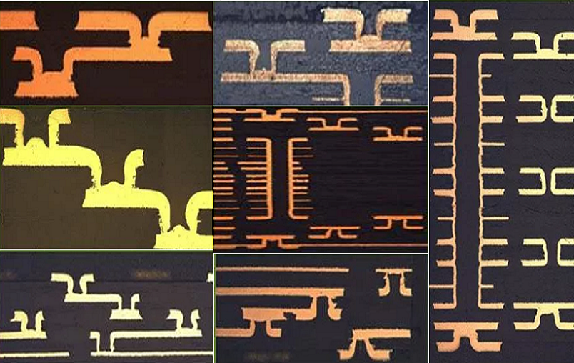
HDI PCB Structure Types
Core Architecture Fundamentals
HDI PCB types follow a build-up construction model where dielectric and copper layers are added incrementally to a central core.
- Build-up layers: Thin dielectric layers ≤100μm with laser-drilled microvias
- Core layer: Standard rigid dielectric providing mechanical stability
- Lamination cycles: 1 to 4+ sequential bonding operations
- Compliance: All structures adhere to IPC-2226 and IPC-6012 Class 2/3
Naming Convention (M+N+M)
The universal HDI naming structure defines build-up layers on each side of a core:
- M = number of build-up layers per side
- N = number of core layers
- Examples: 1+N+1, 2+N+2, 3+N+3, Any-Layer ALI
Common HDI PCB Classifications
Basic HDI (1+N+1)
Single build-up layer on both sides of a central core.
- Entry-level HDI structure
- Single lamination cycle
- Blind microvias connecting outer to adjacent inner layers
- Minimum trace width: 100μm (4mil)
- Microvia diameter: 100–150μm
- Cost-effective for consumer electronics
Advanced HDI (2+N+2 / 3+N+3)
Multiple build-up layers on both sides of the core.
- 2 or 3 sequential lamination cycles
- Stacked and staggered microvias enabled
- Minimum trace width: 75μm (3mil)
- Supports 0.3–0.4mm pitch BGA components
- Used in 5G, automotive, and high-performance computing
Any-Layer Interconnect
Full-build HDI structure with no conventional core.
- Laser microvias connecting any two layers
- Maximum routing density
- Ultra-thin profile down to 0.4mm
- Minimum trace width: 50μm (2mil)
- Used in premium mobile and wearable devices
Learn more about: What is HDI PCB? A Complete Guide for Beginners to High-Density Interconnect
IPC-2226 Structure Types
Type I (1+N+1)
Single microvia layer on one or both sides of a core.
- Uses blind microvias and through-hole vias
- No buried vias permitted
- Aspect ratio ≤1:1
- Entry-level hdi circuit boards for basic miniaturization
Type II (1+N+1)
Single microvia layer on one or both sides of a core.
- Uses blind, buried, and through-hole vias
- Higher routing density than Type I
- Supports moderate component pin counts
- Balances performance and cost
Type III (2+N+2 or higher)
Two or more microvia layers on one or both sides of a core.
- Stacked and staggered microvia configurations
- Maximum interconnection density
- Supports fine-pitch components
- High-speed signal integrity optimized
Types IV–VI
Extended structures for specialized high-complexity applications.
- Multi-level stacked microvias
- Coreless and partial-core constructions
- Ultra-fine line capabilities ≤50μm
- Used in aerospace and premium electronics
Build-up Technology (M+N+M)
1+N+1 HDI Structure
- 1 build-up layer top and bottom
- 1 sequential lamination cycle
- Blind microvias: 100–150μm
- Core thickness: 0.4–1.0mm
- Total layers: 4 to 12 typical
- Cost: Lowest HDI tier
i+N+i HDI Structure
- Variable build-up layers (i=2,3) top and bottom
- 2–3 lamination cycles
- Stacked microvias up to 3 levels
- Dielectric thickness: 50–75μm per layer
- Total layers: 8 to 20 typical
- Supports complex BGA escape
Any Layer HDI
- No traditional core structure
- All layers interconnected by microvias
- 4+ lamination cycles
- Aspect ratio ≤0.75:1
- Minimum via diameter: 75μm
- Ultra-high-density routing
Via Structures in HDI
Stacked Vias
Vertically aligned microvias forming a continuous conductive path.
- Vertical alignment tolerance: ±25μm
- Copper-filled for structural stability
- Maximum stack height: 3 build-up layers
- Reduces lateral space consumption by 60%
- Risk: Plating voids with improper processing
Staggered Vias
Offset microvias between adjacent build-up layers.
- Offset distance: ≥50μm
- Lower processing risk than stacked vias
- Easier plating uniformity
- Higher lateral space requirement
- Preferred for high-reliability applications
Skip Vias
Microvias spanning two non-adjacent build-up layers.
- Eliminates intermediate landing pads
- Aspect ratio ≤0.8:1
- Reduces routing layers by 1–2 layers
- Advanced laser drilling capability required
- Factory yield: 92–95% with controlled parameters
Learn more about: How to Choose Between Microvias, Stacked Vias, and Staggered Vias for High Density Interconnect (HDI) PCBs
Key HDI Features & Benefits
Fine Line Capability
- Type I: Minimum trace width/spacing 100/100μm
- Type II: Minimum trace width/spacing 75/75μm
- Type III: Minimum trace width/spacing 50/50μm
- Any-Layer: Minimum trace width/spacing 40/40μm
- Etching tolerance: ±10μm for all HDI types
Microvia Performance
- Diameter range: 75–150μm
- Aspect ratio: ≤1:1 (industry best practice)
- Pull strength: ≥1.5kgf per microvia
- Thermal cycling: 1000 cycles (-40°C to 125°C)
- Resistance: ≤5mΩ per via
Comparison Tables
HDI Type Comparison (IPC-2226)
| IPC Type | Structure | Lamination Cycles | Microvia Types | Min Trace |
|---|---|---|---|---|
| Type I | 1+N+1 | 1 | Blind | 100μm |
| Type II | 1+N+1 | 1 | Blind + Buried | 100μm |
| Type III | 2+N+2 | 2 | Stacked + Staggered | 75μm |
| Any-Layer | ALI | 4+ | All Layer-to-Layer | 50μm |
Via Structure Comparison
| Via Type | Space Usage | Processing Risk | Yield Rate | Best For |
|---|---|---|---|---|
| Stacked | Minimal | Medium | 91–94% | Ultra-dense designs |
| Staggered | Moderate | Low | 96–98% | High reliability |
| Skip | Efficient | High | 89–92% | Layer reduction |
Core Technical Parameters
Type I HDI
- Trace width/spacing: 100/100μm
- Microvia diameter: 125–150μm
- Aspect ratio: ≤1:1
- Dielectric thickness: 75–100μm
- Impedance tolerance: ±5%
- Registration accuracy: ±50μm
Type II HDI
- Trace width/spacing: 75/75μm
- Microvia diameter: 100–125μm
- Aspect ratio: ≤0.9:1
- Dielectric thickness: 50–75μm
- Impedance tolerance: ±4%
- Registration accuracy: ±40μm
Type III HDI
- Trace width/spacing: 50/50μm
- Microvia diameter: 75–100μm
- Aspect ratio: ≤0.8:1
- Dielectric thickness: 40–50μm
- Impedance tolerance: ±3%
- Registration accuracy: ±30μm
Case Study
Project Specifications
- HDI Type: 2+8+2 (Type III)
- Application: 5G small cell module
- Layers: 12 total
- Features: Stacked microvias 100μm, 75μm traces
- Impedance: 50Ω ±3%
- Component pitch: 0.4mm BGA
Issues Encountered
- Initial stacked via registration error ±40μm
- Trace etching tolerance ±15μm out of spec
- Microvia voiding in bottom 15% of vias
- Warpage 0.35mm/m exceeding limits
Improvements Implemented
- Laser drilling alignment calibration ±20μm
- Etch factor compensation for fine lines
- Aspect ratio reduced to 0.75:1
- Symmetric stack-up optimization
- Controlled lamination pressure profile
Results
- Registration accuracy improved to ±25μm
- Trace tolerance stabilized to ±8μm
- Microvia voiding eliminated
- Warpage controlled to 0.18mm/m
- Manufacturing yield improved from 76% to 95.8%
- Module size reduced by 32%
Common Design Errors
- Exceeding microvia aspect ratio: Ratio >1:1 causes plating voids and 10–20% yield loss
- Insufficient staggered via spacing: <50μm offset causes short circuits and rework
- Unbalanced stack-up: Creates warpage >0.3mm/m leading to assembly failure
- Trace width below process capability: <50μm without advanced equipment causes opens
- Missing microvia copper fill: BGA pad dimpling >25μm causes solder defects
Quality Control & Compliance
Testing Protocols
- Microvia cross-section: Void percentage <2%
- Impedance testing: TDR measurement per IPC-TM-650
- Automated optical inspection: 100% trace and via coverage
- Laser drill verification: Diameter and position accuracy
- Solderability testing: IPC-6012 Class 3 compliance
Standards Compliance
- IPC-2226: HDI PCB design standard
- IPC-2315: Microvia design guidelines
- IPC-6012: Rigid PCB performance specification
- IPC-4103: High-speed laminate requirements
- ISO 9001: Manufacturing quality system
FAQ
Q1: What are the main HDI PCB types defined by IPC-2226?
A1: IPC-2226 defines Type I, Type II, Type III, and extended Types IV–VI. Type I/II use 1+N+1, Type III uses 2+N+2 or higher, and IV–VI support advanced coreless structures.
Q2: What is the difference between stacked and staggered microvias?
A2: Stacked vias align vertically for minimal space; staggered vias offset horizontally for lower processing risk and higher reliability in hdi pcb manufacturing.
Q3: What does 2+N+2 mean in HDI PCB types?
A3: 2+N+2 indicates two build-up layers on both sides of a central core, requiring two sequential lamination cycles and supporting stacked microvias.
Q4: When should Any-Layer HDI be used instead of standard HDI types?
A4: Any-Layer HDI enables maximum miniaturization, supports 0.3mm pitch components, and reduces layer count by 30–50% for ultra-compact consumer and wearable devices.
If you need SBU HDI PCB manufacturing or design support, our engineering team provides free DFM analysis and quotation.


