
HDI PCB vs Standard PCB: Definitive Engineering Differences
Electronic engineers and procurement teams face constant decisions between high density interconnect (HDI) and standard printed circuit boards. Standard PCBs remain viable for simple applications, but modern tech projects—from AI servers to wearable medical devices—demand the precision and density of HDI boards. Choosing incorrectly leads to compromised performance, oversized designs, or unnecessary cost overruns. This guide breaks down the technical, manufacturing, and practical differences from a factory engineer’s perspective, providing actionable data for informed selection.
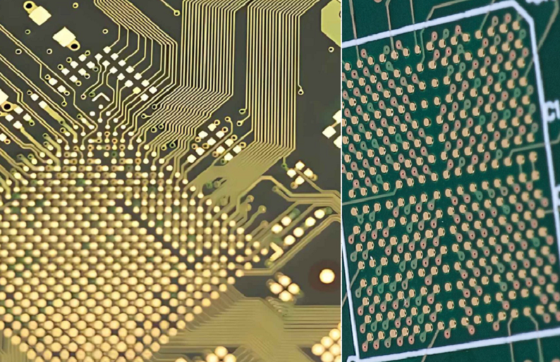
Learn more about: How to Design HDI Microvia PCB
HDI PCB Key Characteristics & Capabilities
Core Physical & Design Specifications
HDI PCBs are defined by micron-scale features and advanced layer structures that enable superior performance. Per IPC-6016, these boards meet strict dimensional standards:
- Trace Dimensions: Fine line/spacing combinations as tight as 20μm/20μm for advanced UHDI designs; 30μm/30μm for standard HDI production
- Microvia Specifications: Laser-drilled microvias with diameters from 25μm to 150μm, aspect ratios limited to 1:1 for reliable plating
- Layer Configurations: Utilizes sequential lamination structures including 1+N+1 (single build-up), 2+N+2 (double build-up), and ELIC (Any-Layer Interconnect) designs
- Copper Weights: Ranges from ½ oz (17.5μm) for fine-trace layers to 2 oz (70μm) for power/ground planes
- Impedance Control: Maintains 50Ω single-ended and 100Ω differential impedance with ±5% tolerance (±2% for high-speed applications)
- Material Systems: High-Tg laminates (Tg ≥170°C), low-loss dielectrics (Df ≤0.008), and specialized flex-rigid materials for multi-technology applications
Performance & Manufacturing Capabilities
The engineering value of HDI PCBs lies in their ability to deliver advanced functionality in compact form factors:
- Wiring Density: Supports 120-160 pins per square inch and 200-300 traces per square inch—2-4 times higher than standard PCBs
- Signal Integrity: Enables data rates up to 50Gbps through shorter signal paths (30-50% reduction vs. standard PCBs) and minimal stubs
- Thermal Management: Copper-filled microvias and thermal via arrays dissipate heat at 15W/cm², 87% higher than standard PCBs
- Manufacturing Processes: Employs laser drilling (12,000+ vias per second), modified semi-additive process (mSAP) for fine traces, and vacuum via filling for 100% reliability
- Component Compatibility: Accommodates fine-pitch components down to 0.2mm BGA/QFN pitches, critical for high-pin-count integrated circuits
Standard PCB Key Characteristics & Capabilities
Core Physical & Design Specifications
Standard PCBs, also known as conventional PCBs, are defined by larger features and simpler structures suitable for low-density applications:
- Trace Dimensions: Minimum line/spacing of 100μm/100μm for standard production; 75μm/75μm for high-end standard designs
- Via Specifications: Mechanical-drilled through-holes with diameters ≥200μm, requiring annular rings of at least 15μm
- Layer Configurations: Typically 2-8 layers using batch lamination with thicker dielectric layers (≥100μm)
- Copper Weights: Common range from 1 oz (35μm) to 2 oz (70μm); thinner copper (½ oz) used only for specific low-current applications
- Impedance Control: Basic impedance management with ±10% tolerance; limited capability for high-speed signal integrity
- Material Systems: Standard FR-4 laminates (Tg 130-140°C), with limited material options for extreme environments
Performance & Manufacturing Capabilities
Standard PCBs deliver reliable performance for applications without extreme density or speed requirements:
- Wiring Density: Supports 40-80 pins per square inch and 80-120 traces per square inch
- Signal Integrity: Suitable for signal speeds up to 10Gbps; longer signal paths increase latency and crosstalk risks
- Thermal Management: Dissipates heat at 8W/cm², requiring additional thermal solutions for high-power applications
- Manufacturing Processes: Relies on subtractive etching, mechanical drilling, and batch lamination—processes with established yields ≥95% for simple designs
- Component Compatibility: Works with standard component pitches ≥0.8mm; incompatible with advanced fine-pitch ICs
Core Difference Comparison
Technical Specifications Comparison
| Parameter | HDI PCB | Standard PCB | Critical Engineering Impact |
|---|---|---|---|
| Minimum Trace/Space | 20μm/20μm (advanced) | 100μm/100μm (standard) | 4x higher routing density for HDI |
| Minimum Via Size | 25μm (microvia) | ≥200μm (through-hole) | 70% space reduction for HDI interconnections |
| Layer Count (Equivalent Functionality) | 4-6 layers | 8-10 layers | 30-40% thinner profile for HDI |
| Component Pitch Support | Down to 0.2mm | ≥0.8mm | Enables advanced IC integration for HDI |
| Signal Speed Capacity | Up to 50Gbps | ≤10Gbps | Supports AI/5G technologies only with HDI |
| Thermal Dissipation | 15W/cm² | 8W/cm² | Better heat management for high-power HDI designs |
Manufacturing & Cost Comparison
- Production Complexity: HDI requires specialized laser drilling equipment, sequential lamination, and mSAP processes—increasing setup costs by 30-50%
- Material Usage: HDI uses thinner dielectric layers (30-50μm) and specialized high-Tg materials, raising per-square-inch costs by 20-30%
- Yield Rates: Standard PCBs achieve 95-98% yield for simple designs; HDI yields range 92-96% for volume production, with higher scrap rates for complex UHDI
- Assembly Complexity: HDI demands high-accuracy placement equipment (±1μm) and specialized rework tools, increasing assembly costs by 25-35%
- Total Project Cost: HDI may have 20-30% higher material costs but often delivers 15-20% lower total costs through reduced board size, fewer components, and simplified assembly
Learn more about: Cost Differences Between 1+N+1, 2+N+2, and Any-Layer High Density Interconnect (HDI) PCBs
| Comparison Dimension | HDI PCB | Standard PCB |
|---|---|---|
| Production Complexity | Specialized laser drilling/sequential lamination (30-50% higher setup cost) | Basic mechanical drilling/batch lamination (low setup cost) |
| Material Usage Cost | 20-30% higher per-square-inch cost (specialized high-Tg materials) | Lower cost (standard FR-4, thicker dielectrics) |
| Yield Rates (Volume Production) | 92-96% (complex UHDI lower at 85-90%) | 95-98% (simple designs) |
| Assembly Cost | 25-35% higher (±1μm placement accuracy required) | Lower (±5μm placement tolerance sufficient) |
| Total Project Cost | 15-20% lower (smaller size/fewer components) | Higher for high-density designs (larger board/more layers) |
Suitability for High-Technology Industries
Industry-Specific HDI PCB Applications
HDI PCBs are the foundation of California’s cutting-edge technology sectors, delivering the performance required for innovation:
- AI & Data Centers: Power AI training servers with 25Gbps+ data rates, high-layer-count boards (up to 36 layers), and thermal management for GPU-intensive applications
- Consumer Electronics: Enable smartphone and wearable innovation through miniaturization (50% size reduction) and integration of high-pin-count processors
- Medical Devices: Provide biocompatible solutions for diagnostic equipment, implants, and monitoring devices with ultra-thin profiles (≤0.4mm) and 100% reliability
- Automotive: Support ADAS systems, infotainment, and EV powertrains with high-Tg materials (Tg ≥180°C) and resistance to extreme thermal cycling (-40°C to +125°C)
- Aerospace & Defense: Deliver radiation-hardened solutions for satellite communications and military systems withstanding harsh environmental conditions
ndustry-Specific Standard PCB Applications
Standard PCBs remain viable for applications without extreme density or performance demands:
- Industrial Controls: Provide cost-effective solutions for basic automation and control systems with moderate component counts
- Power Supplies: Deliver reliable power conversion for low-to-medium power applications without high-speed signal requirements
- Low-Cost Consumer Products: Serve basic electronics with minimal functionality and density needs
- Legacy Systems: Maintain compatibility with older component libraries and manufacturing infrastructure
Real Factory HDI vs Standard PCB Case Study
Project Overview & Initial Parameters
A California aerospace manufacturer required a PCB upgrade for a satellite communication terminal. The original design used an 8-layer standard PCB, but performance limitations led to a redesign with a 6-layer HDI PCB.
- Original Standard PCB Specs: 8 layers, 100μm/100μm trace/space, 250μm through-holes, 1.6mm thickness, standard FR-4 (Tg 130°C)
- HDI Redesign Specs: 6 layers, 30μm/30μm trace/space, 80μm microvias, 1.0mm thickness, high-Tg FR-4 (Tg 170°C)
- Production Target: 500 units annually, weight reduction ≥30%, signal speed upgrade to 25Gbps
Manufacturing Challenges & Root Causes
The transition revealed three key differences impacting production:
- Microvia Plating Voids (10% initial defects): Vacuum filling pressure at 40psi created 5-8% voids in microvias, failing IPC-6016 standards
- Trace Etching Variation (8% defects): Subtractive process couldn’t maintain 30μm trace width with ±5μm tolerance
- Layer Registration Error (6% defects): Batch lamination produced ±15μm misalignment between build-up layers
Implemented Solutions & Quantified Results
- Vacuum Filling Optimization: Increased pressure to 75psi, implementing stage-wise filling to achieve 100% void-free microvias (X-ray verified)
- Process Switch to mSAP: Modified semi-additive process reduced trace width variation to ±3μm, meeting IPC-6012 Class 3 requirements
- Sequential Lamination Adoption: Layer-by-layer lamination improved registration accuracy to ±8μm
Final Results: 95% production yield, 35% weight reduction, 2.5x higher signal speed capability. Material costs increased by 18%, but total project costs decreased by 12% due to fewer components and simplified assembly.
Common Design Errors (Production End Perspective)
HDI PCB Design Mistakes
- Exceeding Microvia Aspect Ratio: Designing vias with aspect ratio >1:1 causes uneven plating and voids (70% of HDI manufacturing failures)
- Inadequate Solder Mask Dams: <15μm dams between fine-pitch pads lead to bridging (20μm minimum required for 0.2mm pitch components)
- Unfilled Vias Under Components: Microvias under BGAs/QFNs cause solder wicking and assembly yield reduction by 30%
- Ignoring Laser Drilling Constraints: Designing microvias <50μm for factories without UV laser capability (minimum 50μm for volume production)
- Asymmetric Stackup Design: Uneven copper distribution causes >0.75% warpage (IPC-6016 limit), leading to SMT placement failure
Standard PCB Design Mistakes
- Overspecifying Density: Designing 75μm/75μm trace/space for standard PCB production increases costs by 25% without performance benefit
- Neglecting Thermal Management: Lack of ground planes and thermal vias leads to overheating in medium-power applications
- Excessive Layer Count: Adding unnecessary layers increases thickness by 50% and cost by 40% for simple designs
- Poor Via Placement: Crowded through-holes reduce routing options and increase manufacturing complexity
FAQ – HDI vs Standard PCB Selection
1. What factors determine whether to use HDI or standard PCB?
Select HDI PCB if your design requires: component pitch ≤0.8mm, board size <100cm², signal speed >10Gbps, or layer count reduction (replace 8+ conventional layers with 4-6 HDI layers). Choose standard PCB for simple designs (component pitch ≥1.0mm, low signal speed) where cost-effectiveness is the primary priority.
2. How do the manufacturing processes differ between HDI and standard PCBs?
Standard PCBs use subtractive etching, mechanical drilling, and batch lamination—processes with lower equipment requirements and higher yields for simple designs. HDI PCBs require laser drilling, sequential lamination, and modified semi-additive processes (mSAP) for fine traces, demanding specialized machinery and higher process control standards.
3. What are the cost implications of choosing HDI over standard PCB?
HDI PCBs have 20-30% higher per-square-inch material costs and 25-35% higher assembly costs. However, total project costs are often lower (10-20% savings) due to 30-50% smaller board sizes, 30% fewer components, and simplified assembly. For high-volume production (100k+ units), the cost difference narrows to 5-10%.
4. How do HDI and standard PCBs compare in terms of reliability?
HDI PCBs offer superior reliability through better signal integrity, thermal management, and resistance to environmental stressors. They maintain performance through 500+ thermal cycles (-40°C to +125°C) and support higher current densities. Standard PCBs provide reliable performance for their intended applications but may require additional design considerations for high-power or high-speed environments.
If you need HDI PCB manufacturing or design support,our engineering team provides free DFM analysis and quotation.


![Understanding PCB Costs & Pricing [Your Complete Guide]](https://hdicircuitboard.com/wp-content/uploads/elementor/thumbs/Understanding-PCB-Costs-Pricing-Your-Complete-Guide-qzzhe6mcaxuolkux3xalfktgavumi9y1aqfbs9bpv4.webp "Understanding PCB Costs & Pricing [Your Complete Guide]")


