
HDI PCB and standard PCB represent two distinct fabrication architectures: high-density interconnect (HDI) boards use microvias, sequential lamination, and fine-line features to achieve ultra-high routing density, while standard PCBs rely on through-hole vias, single-lamination processes, and larger geometries for general-purpose applications. This factory-verified comparison provides quantifiable parameters, structural differences, manufacturing constraints, and application suitability to support engineering selection between hdi pcb and standard printed circuit board platforms.
Learn more about: What is HDI PCB? A Complete Guide for Beginners to High-Density Interconnect
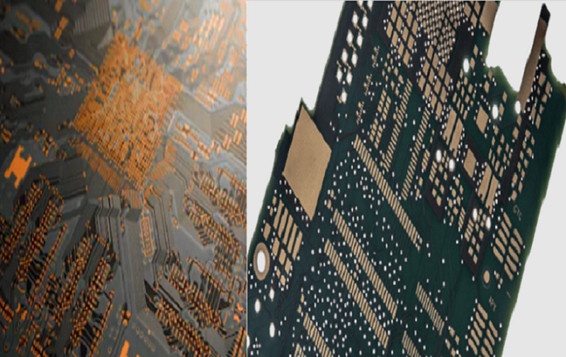
HDI PCB vs Standard PCB: Core Definitions
High-Density Interconnect (HDI) PCB
HDI PCB is an advanced interconnect structure defined by IPC-2226, featuring line width/spacing ≤100μm, microvias ≤150μm, pad density >20 pads/cm², and blind/buried microvia structures.
- Build-up layers with sequential lamination
- Laser-drilled microvias and via-in-pad plating
- Fine-line traces and narrow spacing for high routing density
- Compliant with IPC-2226 and IPC-6012 Class 3 specifications
Standard PCB
Standard PCB refers to conventional rigid boards using mechanical drilling, through-hole vias, and single-step lamination, with minimum features above HDI thresholds.
- Through-hole vias connecting all layers
- Single lamination cycle for full layer stack
- Larger trace width and via geometries
- Compliant with IPC-2221 generic design standards
Key Differences
Via Technology
HDI PCB Via Structures
- Laser-drilled microvias: 100–150μm diameter
- Blind vias, buried vias, stacked microvias
- Via-in-pad with copper fill for BGA escape
- Aspect ratio ≤1:1 for reliable plating
- Elimination of through-hole via stub effects
Learn more about: What is Via-in-Pad? HDI PCB Benefits & Manufacturing Process
Standard PCB Via Structures
- Mechanically drilled through-hole vias: ≥300μm diameter
- Limited blind/buried via capability
- No via-in-pad or microvia stacking
- Aspect ratio up to 10:1
- Stub-related discontinuities in high-speed paths
Density & Space Utilization
HDI PCB Density Features
- Trace width/spacing: 75–100μm (3–4mil)
- Pad density: >20 pads/cm²
- Component pitch support: 0.3–0.5mm BGA
- Footprint reduction: 30–50% vs standard PCB
- Layer count reduction: 30–50% for equivalent routing
Standard PCB Density Features
- Trace width/spacing: ≥150μm (6mil)
- Pad density: ≤15 pads/cm²
- Component pitch support: ≥0.5mm limited BGA
- Larger form factor and greater layer count
- Lower routing efficiency per unit area
Learn more about: Minimum Trace Width, Spacing, and Microvia Size for High Density Interconnect (HDI) PCB Mass Production
Manufacturing Processes
HDI PCB Manufacturing
- Sequential lamination: 1–4 build-up cycles
- Laser drilling for microvia formation
- Via-in-pad copper filling and planarization
- Plasma desmear and advanced metallization
- Tighter registration: ±50μm layer-to-layer
Standard PCB Manufacturing
- Single lamination cycle for full stack
- Mechanical drilling only
- No via filling or specialized planarization
- Conventional desmear processes
- Standard registration: ±75μm layer-to-layer
Performance Comparison
Electrical Performance
HDI PCB Electrical Advantages
- Signal path length reduction: 60–80%
- Parasitic inductance reduction: 50–70%
- Insertion loss improvement: 25–35% at 10GHz+
- Impedance stability: ±5% per IPC-2221 Class 3
- Superior EMI suppression and signal integrity
Standard PCB Electrical Characteristics
- Longer signal paths and higher parasitic effects
- Higher insertion loss at high frequencies
- Impedance variation: ±10% typical
- Increased crosstalk and EMI radiation
- Limited performance above 5Gbps
Mechanical & Reliability Performance
HDI PCB Mechanical Properties
- Thickness reduction: 25–40% vs standard PCB
- Warpage control: ≤0.2mm/m for symmetric structures
- Thermal cycling stability: 1000 cycles -40°C to 125°C
- Enhanced resistance to vibration and shock
Standard PCB Mechanical Properties
- Greater overall thickness and weight
- Warpage typical: ≤0.5mm/m
- Lower thermal cycling reliability margin
- Larger via structures prone to fatigue failure
Application Suitability
HDI PCB Target Applications
- Mobile and wearable electronics
- 5G/6G communication modules
- Automotive ADAS and infotainment
- High-performance computing and AI accelerators
- Medical devices and portable diagnostics
Standard PCB Target Applications
- Industrial control systems
- Consumer appliances and low-speed electronics
- Power distribution and non-critical controls
- Low-speed communication interfaces
- Cost-sensitive general-purpose electronics
Summary Table: HDI PCB vs Standard PCB
| Parameter | Standard PCB | HDI PCB | Performance Gain |
|---|---|---|---|
| Minimum Trace Width | ≥150μm (6mil) | ≤100μm (4mil) | 50% finer features |
| Minimum Via Diameter | ≥300μm (12mil) | ≤150μm (6mil) | 50% smaller vias |
| Interconnection Density | ≤15 pads/cm² | ≥20 pads/cm² | 33% higher density |
| Layer Count Requirement | High | 30–50% Lower | Reduced complexity |
| Signal Loss at 10GHz | High | 25–35% Lower | Improved SI |
| Board Footprint | Standard | 30–50% Smaller | Greater miniaturization |
| Manufacturing Process | Single lamination | Sequential lamination | Advanced fabrication |
| High-Speed Support | ≤5Gbps | ≤112Gbps | Superior high-speed capability |
Technical Parameters
HDI PCB Specifications
- Trace width/spacing: 75–100μm (3–4mil)
- Microvia diameter: 100–150μm (4–6mil)
- Aspect ratio: ≤1:1
- Dielectric thickness: 50–100μm
- Impedance tolerance: ±5%
- Registration accuracy: ±50μm
- Warpage limit: ≤0.2mm/m
Standard PCB Specifications
- Trace width/spacing: ≥150μm (6mil)
- Via diameter: ≥300μm (12mil)
- Aspect ratio: up to 10:1
- Dielectric thickness: ≥100μm
- Impedance tolerance: ±10%
- Registration accuracy: ±75μm
- Warpage limit: ≤0.5mm/m
Case Study
Project Specifications
- Comparison: 12-layer standard PCB vs 8-layer HDI PCB
- Application: Industrial communication processor
- Data rate: 10Gbps Ethernet
- Component: 0.4mm pitch FPGA
Issues with Standard PCB
- Required 12 layers for complete routing
- Through-hole vias caused 38% excess insertion loss
- Warpage at 0.55mm/m prevented automated assembly
- Impedance deviation ±11% out of tolerance
HDI PCB Implementation
- 2+4+2 symmetric HDI stack-up
- 120μm laser microvias and via-in-pad
- 8mil trace width with 4mil spacing
- Sequential lamination with tight dielectric control
Results
- Routing completed in 8 layers vs 12 layers
- Insertion loss reduced by 31%
- Warpage controlled to 0.18mm/m
- Impedance stabilized to ±4.3%
- Manufacturing yield improved from 74% to 95.6%
- Board size reduced by 37%
Common Design Errors
Standard PCB Design Errors
- Overlooking via aspect ratio limits exceeding 10:1 causing plating failures
- Insufficient clearance increasing short-circuit risks in mass production
- Asymmetric stack-up creating warpage exceeding assembly thresholds
- Inadequate power-ground plane spacing reducing noise immunity
HDI PCB Design Errors
- Microvia aspect ratio >1:1 resulting in 15–22% yield loss
- Missing via-in-pad filling causing BGA soldering defects
- Exceeding lamination cycle limits reducing structural reliability
- Insufficient trace clearance violating 3W rule and increasing crosstalk
Quality Control & Compliance
Testing Protocols
- Microvia cross-section analysis for void-free plating
- Impedance testing via TDR per IPC-TM-650
- Automated optical inspection for line width uniformity
- Thermal cycling validation for reliability qualification
Standards Compliance
- HDI PCB: IPC-2226, IPC-2315, IPC-6012 Class 3
- Standard PCB: IPC-2221, IPC-6012 Class 2
- Material compliance: IPC-4103 for high-performance substrates
FAQ
Q1: What is the primary structural difference between HDI PCB and standard PCB?
A1: HDI PCB uses laser-drilled microvias, sequential lamination, and fine-line features, while standard PCB uses mechanically drilled through-hole vias and single-step lamination with larger geometries.
Q2: When should I select HDI PCB instead of standard PCB?
A2: Choose HDI PCB for designs requiring 0.3–0.5mm pitch components, high-speed signals above 5Gbps, miniaturization, or layer count reduction. Standard PCB suffices for low-speed, cost-sensitive applications.
Q3: How does manufacturing differ between HDI PCB and standard PCB?
A3: HDI PCB requires laser drilling, sequential lamination, via-in-pad filling, and tighter registration. Standard PCB uses conventional mechanical drilling and single lamination with simpler processes.
Q4: What performance advantages does HDI PCB provide over standard PCB?
A4: HDI PCB offers 30–50% smaller footprint, 25–35% lower insertion loss, 50–70% reduced inductance, better signal integrity, and supports higher pin-density components than standard PCB.
If you need SBU HDI PCB manufacturing or design support, our engineering team provides free DFM analysis and quotation.


