
High Density Interconnect (HDI) PCBs: The Definitive Guide to Characteristics, Functionality, Benefits & Uses
High density interconnect (HDI) printed circuit boards have become the backbone of modern electronics, addressing the critical need for smaller, more powerful devices. Unlike traditional PCBs, HDI PCBs pack more functionality into compact form factors while enhancing performance and reliability. This guide breaks down their core characteristics, working principles, key benefits, and real-world applications to help you understand their role in advanced electronics.
HDI PCB Characteristics: What Defines High Density Interconnect Technology
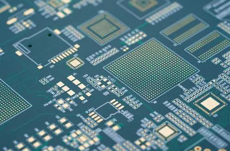
HDI PCBs are distinguished by precise technical specifications and structural features that enable their high-performance capabilities. These characteristics align with industry standards such as IPC-2226, IPC-4104, and IPC-6016, ensuring consistency and reliability across manufacturing.
Core Technical Specifications (Per IPC Standards)
- Line and Space Dimensions: ≤100 µm (0.10mm) for finer wiring density compared to traditional PCBs
- Via Sizes: Microvias with diameter <150 µm (0.15mm), significantly smaller than mechanical drill holes
- Capture Pads: ≤400 µm (0.40mm) to accommodate dense component placement
- Connection Pad Density: >20 pads/cm², enabling more interconnections per unit area
- Aspect Ratio: Microvias maintain an aspect ratio ideally <1 (some manufacturers support up to 2 for stacked microvias)
Structural Features
- Via Technologies: Utilizes blind vias (connect outer layer to inner layers), buried vias (connect inner layers only), and microvias (laser-drilled for layer-to-layer connections)
- Via Configurations: Includes stacked microvias, staggered microvias, and via-in-pad designs for maximum density
- Layer Configurations: Common structures include 1+n+1 (single microvia layer on core sides), 2+n+2 (two microvia layers), and ELIC (Every Layer Interconnection) for full layer interconnectivity
- Material Selection: Uses advanced dielectrics such as photosensitive liquid/dry film dielectrics, polyimide flexible film, resin-coated copper (RCC) foil, and low-loss FR-4 variants
- Manufacturing Processes: Relies on laser drilling, sequential lamination, and precision plating to achieve tight tolerances
Key Design Distinctions from Traditional PCBs
| Parameter | HDI PCB | Traditional PCB |
|---|---|---|
| Component Density | >120-160 pins per square inch | <100 pins per square inch |
| Via Type | Microvias, blind/buried vias | Through-holes primarily |
| Drilling Method | Laser drilling (20-150 µm holes) | Mechanical drilling (>6 mils) |
| Layer Count | Fewer layers (e.g., 4-6 layers replacing 8-10 traditional layers) | More layers for equivalent functionality |
| Weight & Size | 33-40% smaller and lighter | Bulkier with larger footprint |
| Pitch Compatibility | Supports 0.20-0.40mm BGA pitch | Limited to ≥0.8mm pitch |
How HDI PCBs Work: Core Mechanisms & Manufacturing Processes
HDI PCBs achieve their high-density capabilities through specialized design principles and manufacturing techniques that optimize space, signal flow, and component integration. Their functionality revolves around efficient layer interconnectivity and precision fabrication.
Fundamental Working Principles
- Layer Interconnectivity: Microvias, blind vias, and buried vias create direct pathways between layers without wasting space on through-holes that penetrate the entire board
- Signal Path Optimization: Shorter trace lengths (enabled by dense component placement) reduce signal flight time, minimizing reflections and crosstalk
- Stackup Design: Sequential lamination builds layers around a core, allowing for controlled impedance and thermal management
- Via-in-Pad Technology: Vias placed directly in component pads eliminate the need for additional routing space, enabling tighter component spacing
HDI PCB Manufacturing Steps
- Material Preparation: Selection of compatible dielectrics and copper foils (e.g., RCC for thin layers) that meet thermal and electrical requirements
- Inner Layer Processing: Etching of copper layers to create conductor patterns, followed by cleaning and inspection
- Laser Drilling: Creation of microvias (20-150 µm) using infrared or ultraviolet lasers for precision depth control
- Via Metallization: Plating of vias with copper (electroless or electroplating) to ensure conductive pathways, with options for copper or epoxy filling
- Sequential Lamination: Layer-by-layer bonding using prepreg, with multiple press cycles to build the stackup
- Outer Layer Processing: Application of solder mask, silkscreen, and final plating (e.g., gold, tin-lead)
- Quality Control: DFM (Design for Manufacturing) checks, impedance testing, and thermal cycle validation per IPC-6016 standards
Critical Design Considerations
- Stackup Planning: Determining layer count based on BGA pin count and signal requirements
- Impedance Control: Matching trace widths and dielectric thickness to achieve target impedance (50Ω, 100Ω differential)
- Thermal Management: Utilizing copper-filled vias and spread-glass prepregs to dissipate heat in high-power applications
- DFM Compliance: Adhering to fabricator capabilities for trace width (≥0.089mm for advanced designs), clearance, and annular ring requirements
Benefits of HDI PCBs: Why They Outperform Traditional PCBs
HDI printed circuit boards offer a range of advantages that address key pain points in electronics design, from space constraints to signal integrity issues. These benefits translate to improved product performance and cost savings.
Performance Enhancements
- Superior Signal Integrity: Shorter trace lengths and reduced via stubs minimize signal loss (insertion loss ≤0.5dB at 10GHz) and electromagnetic interference (EMI)
- Higher Reliability: Microvias with aspect ratio <1 withstand thermal cycling (≥1000 cycles) and mechanical stress better than through-holes
- Faster Signal Transmission: Reduced signal flight time (up to 40% faster than traditional PCBs) supports high-speed protocols (5G, PCIe 4.0)
- Thermal Efficiency: Enhanced heat dissipation through copper-filled vias and thinner dielectrics reduces component operating temperatures by 10-15°C
Design & Cost Advantages
- Miniaturization: 33-40% reduction in board size and weight enables sleeker, more portable devices
- Layer Reduction: Replaces 8-10 layer traditional PCBs with 4-6 layer HDI designs, cutting material costs by 20-30%
- Increased Component Density: 2-4x higher routing density (inches/square inch) than traditional PCBs
- Faster Time-to-Market: Simplified design process and fewer prototyping iterations reduce development time by 15-20%
Versatility & Scalability
- Compatibility with Fine-Pitch Components: Supports BGAs with pitch as low as 0.20mm and high-pin-count ICs
- Flexible Design Options: Coreless constructions and ELIC technology accommodate complex interconnect requirements
- Cross-Industry Adaptability: Works with consumer electronics, medical devices, automotive systems, and aerospace equipment
- Future-Proofing: Scales to support emerging technologies like 5G, IoT, and wearable devices
Applications of HDI PCBs: Where High Density Interconnect Shines
HDI PCBs are integral to industries where size, weight, performance, and reliability are critical. Their ability to pack more functionality into smaller spaces makes them ideal for cutting-edge applications.
Consumer Electronics
- Smartphones & Tablets: ELIC-structured HDI PCBs enable thinner designs with multiple cameras, 5G connectivity, and high-performance processors
- Laptops & Ultrabooks: Reduced weight (15-20% lighter than traditional PCBs) and improved thermal management support compact, powerful devices
- Wearable Technology: Fitness trackers, smartwatches, and VR headsets rely on miniaturized HDI PCBs for extended battery life and multi-sensor integration
- Digital Cameras: Compact form factors with high-resolution sensors and image processors benefit from dense component placement
Medical Devices
- Implantable Devices: Pacemakers, defibrillators, and neurostimulators use biocompatible HDI PCBs for reliable operation in confined spaces
- Diagnostic Equipment: Ultrasound machines, endoscopes, and blood analyzers leverage HDI technology for precise signal processing and miniaturization
- Portable Medical Tools: Handheld diagnostic devices and point-of-care testing equipment benefit from lightweight, high-performance HDI PCBs
- Imaging Systems: CT scanners and MRI machines use HDI PCBs for high-speed data transfer and thermal stability
Automotive & Aerospace
- Automotive Electronics: Advanced driver-assistance systems (ADAS), infotainment systems, and EV controllers use HDI PCBs for space-efficient, reliable performance
- Aerospace Systems: Satellite components, avionics, and defense equipment rely on rugged HDI PCBs that withstand extreme temperatures and vibration
- Unmanned Aerial Vehicles (UAVs): Lightweight HDI PCBs enable longer flight times and integrated sensor systems
- In-Vehicle Networking: Supports high-speed data transfer between vehicle systems (CAN, Ethernet) with minimal signal loss
Industrial & Communication
- 5G Infrastructure: Base stations and routers use HDI PCBs for high-frequency signal handling and dense port configurations
- IoT Devices: Smart sensors, industrial controllers, and connected equipment benefit from compact, low-power HDI designs
- Industrial Automation: PLCs, robotics, and factory automation systems use HDI PCBs for precise control and real-time data processing
- Networking Equipment: Switches, routers, and servers leverage high-density interconnects for improved throughput and reduced latency
FAQ: Common Questions About High Density Interconnect PCBs
What is the difference between HDI PCB and traditional PCB?
HDI PCBs use microvias, blind/buried vias, and laser drilling to achieve higher component density (2-4x) in smaller footprints. Traditional PCBs rely on through-holes, mechanical drilling, and have lower density with larger form factors. HDI also offers better signal integrity and fewer layers for equivalent functionality.
How to choose the right HDI PCB structure?
Select 1+n+1 for low I/O count BGAs, 2+n+2 for higher I/O and smaller pitch components, and ELIC for complex, high-interconnectivity applications. Consider layer count, component pitch, signal requirements, and manufacturing capabilities when choosing a structure.
What standards govern HDI PCB design and manufacturing?
Key standards include IPC-2226 (specifications for HDI structures), IPC-4104 (dielectric material qualifications), IPC-6016 (HDI substrate specifications), and IPC-2315 (microvia design guidelines). Adhering to these standards ensures compatibility and reliability.
Are HDI PCBs cost-effective compared to traditional PCBs?
Yes—while initial manufacturing costs may be higher, HDI PCBs reduce overall costs by replacing multiple traditional PCBs with one, reducing layer count (20-30% material savings), and shortening time-to-market. The total cost of ownership is lower for high-volume production.
What are the key design challenges for HDI PCBs?
Common challenges include maintaining controlled impedance, managing thermal density, ensuring DFM compliance, and optimizing via placement. Working with experienced fabricators and using advanced design software helps address these challenges.
Conclusion: The Future of Electronics with HDI PCBs
High density interconnect (HDI) PCBs have revolutionized electronics design by addressing the critical need for miniaturization without compromising performance. Their unique characteristics—finer lines, smaller vias, and dense component placement—enable the development of smaller, lighter, more powerful devices across industries. From consumer electronics to life-saving medical equipment, HDI printed circuit boards are at the forefront of technological innovation.
As demand for smaller, smarter, and more connected devices grows, HDI technology will continue to evolve, with advancements in material science, manufacturing processes, and design tools. By leveraging the benefits of HDI PCBs—superior signal integrity, reliability, and cost efficiency—engineers can create the next generation of electronic products that meet the demands of today’s market while preparing for tomorrow’s innovations. Whether you’re designing a wearable device, a medical implant, or an automotive system, HDI PCBs offer the performance and flexibility needed to turn complex ideas into reality.


![Understanding PCB Costs & Pricing [Your Complete Guide]](https://hdicircuitboard.com/wp-content/uploads/elementor/thumbs/Understanding-PCB-Costs-Pricing-Your-Complete-Guide-qzzhe6mcaxuolkux3xalfktgavumi9y1aqfbs9bpv4.webp "Understanding PCB Costs & Pricing [Your Complete Guide]")


