
High-Density Interconnect (HDI) PCB is an advanced printed circuit board structure defined by fine-line geometry, microvias, sequential lamination, and high interconnection density, enabling miniaturization, superior signal integrity, and reduced layer counts compared to conventional PCBs. This guide provides factory-aligned definitions, IPC-compliant parameters, structural classifications, and manufacturing rules for hdi pcb used in consumer electronics, automotive, 5G, and high-speed computing systems.
Learn more about: What is HDI PCB? A Complete Guide for Beginners to High-Density Interconnect
High-Density Interconnect PCB: Official Definition
IPC & Industry Standard Definition
High-Density Interconnect (HDI) PCB is a high-density interconnect printed circuit board with minimum feature sizes and interconnection densities exceeding conventional PCB limits, as defined by IPC-2226 and IPC-2315.
- Minimum line width/spacing: ≤0.10 mm (4 mil)
- Microvia diameter: ≤0.15 mm (6 mil)
- Connection density: ≥20 interconnections per cm²
- Structural features: Blind vias, buried vias, via-in-pad, and sequential lamination
- Compliance: IPC-6012 Class 2/3, IPC-2226, IPC-4103
Core Structural Principle
HDI pcb manufacturing uses a build-up sequential lamination process, adding dielectric and conductive layers incrementally rather than laminating all layers at once. Microvias replace large through-hole vias to shorten electrical paths, lower parasitic inductance, and free routing space for hdi circuit boards.
Key Characteristics and Components
Microvias
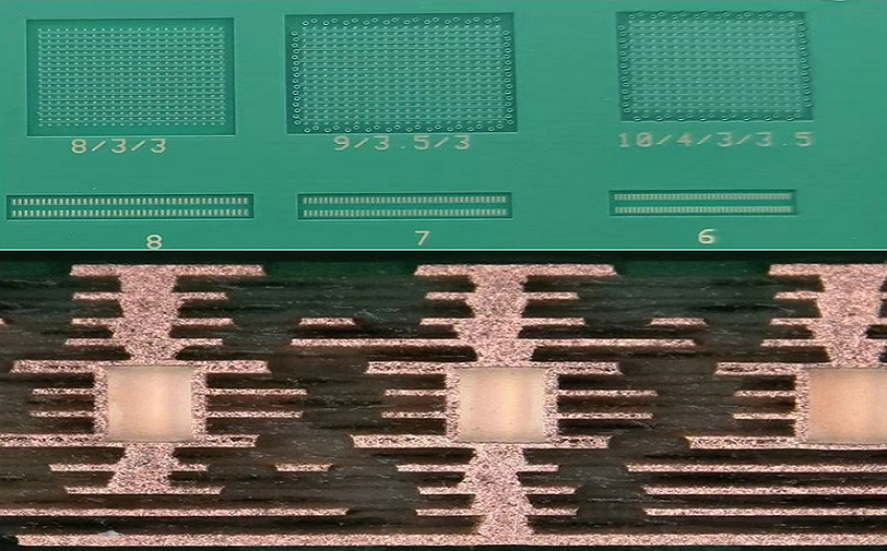
- Laser-drilled microvias: 0.1–0.15 mm diameter, aspect ratio ≤1:1
- Blind vias: Connect outer layer to adjacent inner layer
- Buried vias: Connect inner layers only, no exposure to board surface
- Stacked microvias: Vertically aligned vias for ultra-high-density interconnect
- Fill material: Epoxy resin + copper paste for planarization
Finer Features
- Trace width/spacing: 0.075–0.1 mm (3–4 mil) for high-density routing
- Copper weight: 12–35 μm (0.5–1 oz) for fine-line etching
- Dielectric thickness: 0.05–0.1 mm between layers for impedance control
- Solder mask registration: ±0.05 mm for fine-pitch SMD pads
Via-in-Pad
- Direct via plating within component pad, eliminating fanout routing
- Pad size: 0.2–0.3 mm for 0.3–0.4 mm pitch BGA components
- Void-free copper fill required for reliable soldering
- Reduces trace length by up to 70% in hdi pcb design
Learn more about: What is Via-in-Pad? HDI PCB Benefits & Manufacturing Process
Sequential Lamination
- Progressive layer bonding: Core + 1 build-up layer → lamination → drill → plate → repeat
- Lamination cycles: 1–4 cycles based on HDI order
- Minimizes warpage to ≤0.2 mm/m for high-density interconnect structures
- Enables stacked and staggered microvia configurations
High Pin Density
- Supports components with 0.3–0.5 mm pin pitch
- BGA escape routing without layer count increase
- Up to 4X higher routing density than standard PCBs
- Ideal for high pin-count SoCs, FPGAs, and application processors
Advantages of HDI PCBs
Miniaturization
- 30–50% smaller footprint than standard PCB designs
- 20–40% thinner profile, down to 0.4 mm total thickness
- Eliminates through-hole via land pads for space savings
- Critical for wearables, smartphones, and compact IoT devices
Improved Electrical Performance
- Shortens electrical path length by 60–80%
- Reduces parasitic inductance by 50–70%
- Lowers insertion loss by 25–35% at 10+ GHz
- Enhances signal propagation speed for high-speed SerDes
Reduced Layer Count
- 6-layer HDI replaces 10–12 layer standard PCB
- Lowers material cost by 15–30%
- Simplifies manufacturing and improves yield
- Reduces total board thickness by 25–40%
Better Signal Integrity
- Continuous reference planes minimize impedance discontinuities
- Reduced crosstalk by 20–30% vs. conventional designs
- Impedance control: ±5% (IPC-2221 Class 3)
- Superior EMI suppression and noise immunity
Common Applications
- Mobile & smart devices: Smartphones, tablets, wearables
- Automotive: ADAS, infotainment, EV controllers
- 5G/6G infrastructure: Small cells, RF frontends, antennas
- High-performance computing: Servers, AI accelerators, FPGA modules
- Medical: Portable diagnostics, imaging, implantable devices
- Consumer electronics: VR/AR headsets, IoT sensors, cameras
HDI Classification (Structural Types)
Core + Build-Up Structure
- 1+N+1: 1 build-up layer each side of core (1st order HDI)
- 2+N+2: 2 build-up layers each side (2nd order)
- 3+N+3: 3 build-up layers each side (3rd order)
- N = internal core layer count
Learn more about: HDI PCB Stack Design: 1+N+1, 2+N+2, 3+N+3, 4+N+4 Explained
Any-Layer Interconnect (ALI)
- Full build-up structure without traditional core
- Laser-drilled microvias connecting any two layers
- Maximum routing density for ultra-compact designs
- Used in high-end smartphones and high-density interconnect modules
Key Comparisons
| Parameter | Conventional PCB | HDI PCB | Benefit |
|---|---|---|---|
| Min Trace Width | ≥0.15 mm | ≤0.10 mm | 50% finer routing |
| Min Via Diameter | ≥0.3 mm | ≤0.15 mm | 50% smaller vias |
| Interconnection Density | ≤15/cm² | ≥20/cm² | 33% higher density |
| Layer Count | High | 30–50% Lower | Reduced complexity |
| Signal Loss | High | 25–35% Lower | Better performance |
| HDI Type | Structure | Lamination Cycles | Application |
|---|---|---|---|
| 1st Order | 1+N+1 | 1 | Consumer electronics |
| 2nd Order | 2+N+2 | 2 | Automotive, industrial |
| 3rd Order | 3+N+3 | 3 | High-end mobile, 5G |
| Any-Layer | ALI | 4+ | Ultra-compact designs |
Core Technical Points
- Trace width/spacing: 0.075–0.10 mm (3–4 mil)
- Microvia diameter: 0.10–0.15 mm (4–6 mil)
- Aspect ratio: ≤1:1 for microvias
- Dielectric thickness: 0.05–0.10 mm
- Impedance: 50Ω single-ended, 90–100Ω differential ±5%
- Copper thickness: 12–35 μm (0.5–1 oz)
- Warpage limit: ≤0.2 mm/m
- Registration accuracy: ±0.05 mm layer-to-layer
Case Study
Project Specifications
- Type: 2+N+2 HDI (2nd order), 8 layers
- Application: 5G modem module
- Materials: Low-loss high-frequency laminate
- Features: Microvias 0.12 mm, via-in-pad, 3.5/3.5 mil lines
- Impedance: 50Ω ±5%
Issues Encountered
- Initial design used through-hole vias causing 42% excess inductance
- Trace width too wide, preventing BGA fanout
- Warpage at 0.5 mm/m exceeding assembly limits
- Impedance deviation ±12% out of tolerance
Improvements Implemented
- Converted to 0.12 mm laser microvias and via-in-pad
- Reduced trace width to 0.09 mm (3.5 mil)
- Implemented symmetric 2+4+2 stackup
- Tightened dielectric thickness tolerance to ±0.01 mm
Results
- Impedance stabilized to ±4.2%
- Warpage reduced to 0.18 mm/m
- Routing completed in 8 layers vs. original 12-layer plan
- Manufacturing yield improved from 78% to 96.3%
- Module size reduced by 38%
Common Design Errors
- Overlooking microvia aspect ratio: Ratio >1:1 causes plating voids and 15–22% yield loss
- Insufficient trace clearance: Violating 3W rule increases crosstalk beyond IPC limits
- Asymmetric stackup: Creates warpage >0.3 mm/m leading to assembly failure
- Inadequate via filling: Poor planarization causes solder defects and BGA bridging
- Ignoring registration tolerance: Misalignment >0.075 mm causes open circuits
Quality Control & Compliance
Testing Protocols
- Microvia cross-section inspection: Void rate <2%
- Impedance testing: TDR measurement per IPC-TM-650
- Automated optical inspection (AOI) for line defects
- Thermal cycling: 1000 cycles -40°C to +125°C
- Solderability testing: IPC-6012 Class 3
Standards Compliance
- IPC-2226: HDI design standard
- IPC-2315: Microvia design guidelines
- IPC-6012: PCB performance specification
- IPC-4103: High-frequency laminate requirements
FAQ
Q1: What formally defines a High-Density Interconnect (HDI) PCB?
A1: HDI PCB is defined by IPC standards as a board with trace width/spacing ≤0.10 mm, microvias ≤0.15 mm, connection density ≥20/cm², and using blind/buried vias with sequential lamination.
Q2: What is the difference between 1st, 2nd, and 3rd order HDI?
A2: Order refers to build-up layers: 1+N+1 (1st), 2+N+2 (2nd), 3+N+3 (3rd). Higher order enables finer lines, smaller vias, and greater miniaturization.
Q3: What is via-in-pad and why is it used in HDI PCB?
A3: Via-in-pad places a filled microvia directly within component pads, eliminating fanout routing, shortening paths, and enabling 0.3–0.5mm pitch BGA escape in hdi circuit boards.
Q4: How does HDI PCB differ from standard PCB?
A4: HDI uses microvias, fine lines, sequential lamination, and higher density, reducing size by 30–50%, layers by 30–50%, and improving signal integrity significantly.
If you need SBU HDI PCB manufacturing or design support, our engineering team provides free DFM analysis and quotation.


