- Blind vias, buried vias, Ultra HDI PCB
- High frequency low loss PCB material
- TLY-5, RF35, RF-35TC, TSM-DS3, TLX-8, TLX-9 material
- RO4003, RO4350B, RO4835, RT/duroid 5870, RT/duroid 5880, RT/duroid 6002, TMM3, TMM4, TMM6, TMM10, TMM10i material
High Frequency PCB Solutions | Custom Design & Manufacturing Services
High Frequency PCB Basics & Material Selection
What is High Frequency PCB & Its Industry Standards
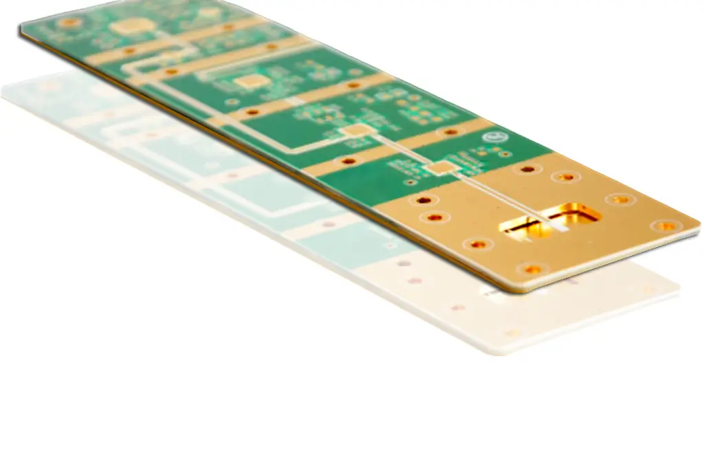
A high frequency PCB—also referred to as a high frequency circuit board—is a specialized printed circuit board engineered to transmit signals with frequencies of ≥500MHz or data rates of ≥1Gbps. Its core attributes include ultra-low dielectric loss (Df≤0.003) and a stable dielectric constant (Dk) across wide temperature ranges, a critical advantage that standard PCBs cannot match. Unlike conventional circuit boards, high frequency PCBs minimize signal attenuation, crosstalk, and phase shift, making them indispensable for 5G telecom base stations, aerospace radar systems, and satellite communication equipment. All our high frequency PCB products adhere strictly to IPC-6012 and IPC-2225 high-frequency-specific standards, with impedance control tolerance locked at ±3% to meet the reliability demands of mission-critical applications.
High Frequency PCB Core Material Options
We offer a proprietary portfolio of three high frequency PCB core materials, tailored to distinct frequency bands and project budget constraints— a selection that sets us apart from generic PCB suppliers:
- PTFE (Polytetrafluoroethylene): Boasting a Dk of 2.2 and Df of 0.0009, this material is optimized for 40GHz+ satellite radar high frequency circuit board projects. It delivers exceptional thermal stability (-200°C to 260°C) and chemical resistance, though its premium performance comes with a higher material cost.
- Rogers Series (RO4350B/RO4003C): With a Dk range of 3.48–3.55 and Df range of 0.0037–0.004, this is the industry’s most widely adopted material for 5G telecom high frequency PCBs. It strikes a perfect balance between high-frequency performance and cost efficiency, making it ideal for mass production of base station modules.
- High-Frequency FR-4: Featuring a Dk of 3.8 and Df of 0.008, this is a cost-effective alternative for 500MHz–6GHz industrial high-frequency devices. It caters to clients with budget limitations and moderate signal integrity requirements, without compromising on basic high-frequency functionality.
High Frequency PCB Custom Design Services
High Frequency PCB Design Guidelines
Our high frequency PCB design service follows five core, high-frequency-exclusive guidelines to guarantee signal integrity and manufacturability:
- Precision Impedance Matching: Design 50Ω (RF applications) or 75Ω (video applications) characteristic impedance with a ±3% tolerance. We use advanced 2D/3D field solvers for simulation before prototyping to eliminate trial-and-error iterations.
- Optimized Trace Routing: Limit trace length to ≤λ/20 (where λ equals signal wavelength) for high frequency PCBs to minimize phase shift. Maintain a spacing of 1.5x the trace width between adjacent traces to completely eliminate crosstalk interference.
- Shielded Ground Plane Design: Add a continuous ground plane directly beneath signal traces to reduce electromagnetic interference (EMI). Space grounding vias at ≤0.1λ intervals to connect ground layers, creating a 360° shielding effect for sensitive high-frequency signals.
- Strategic Component Placement: Position high-frequency chips (e.g., RF transceivers) in close proximity to connectors to shorten signal paths. Place passive components (capacitors/resistors) within 0.5mm of chip pins to enhance decoupling efficiency and reduce noise.
- Low-Reflection Via Design: Replace through-holes with blind/buried vias to shorten stub length to ≤0.5mm, a modification that drastically reduces signal reflection in high frequency circuit board designs.
High Frequency PCB DFM Consulting
Our free high frequency PCB Design for Manufacturing (DFM) consulting service optimizes designs for cost reduction and reliability enhancement, addressing pain points unique to high-frequency PCB manufacturing:
- Material Process Compatibility: Verify that selected substrates align with our lamination and drilling processes. For example, PTFE substrates require specialized laser drilling to prevent delamination during fabrication.
- Ultra-Feature Feasibility Validation: Confirm that ultra-fine lines (≤2mil) and microvias (≤0.1mm) for high frequency PCBs are manufacturable at scale, with zero negative impact on production yield rates.
- Cost Optimization Without Performance Loss: Recommend alternative materials (e.g., switching from Rogers RO4350B to RO4003C) or minor design adjustments (e.g., increasing trace width by 0.5mil) to cut production costs by 10–20% while preserving signal integrity.
All DFM reports include a quantifiable manufacturability score and targeted revision suggestions, reducing design iteration cycles by 30% for high frequency PCB projects.
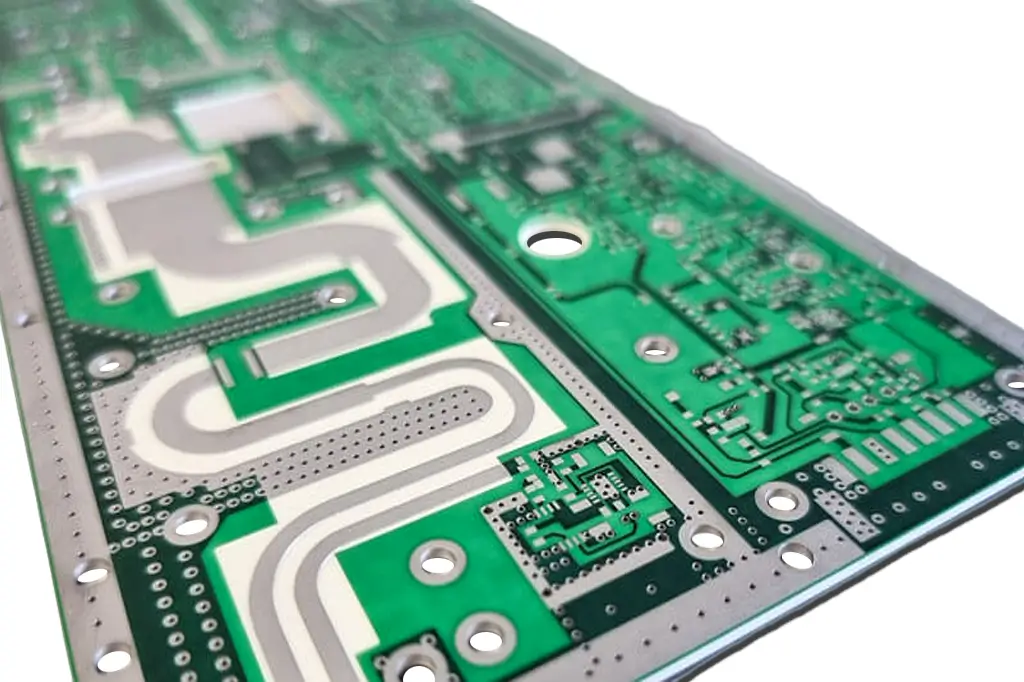
High Frequency PCB Fabrication Processes
High Frequency PCB Impedance Control
Our high frequency PCB fabrication process incorporates four proprietary steps for precision impedance control— a core differentiator that sets us apart from standard PCB manufacturers:
- Pre-Fabrication 3D Simulation: Use industry-leading 3D impedance simulation software to validate the relationship between trace width/space and target impedance (50Ω/75Ω) for selected substrates. For instance, Rogers RO4350B requires an 8mil trace width to achieve 50Ω impedance on a 0.5mm thick substrate.
- Micron-Level Lamination Control: Maintain prepreg thickness tolerance at ±5μm during the lamination process. Even a 1μm thickness variation can cause a 1Ω impedance deviation in high frequency circuit boards, a margin that is unacceptable for high-reliability applications.
- Uniform Pulse Plating: Apply pulse plating technology to copper traces, ensuring plating thickness uniformity of ±2μm. This prevents impedance drift in high-frequency signal paths, a common issue with traditional DC plating methods.
- 100% Post-Fabrication Testing: Conduct full-panel impedance testing using a network analyzer for every high frequency PCB batch. Any board that falls outside the ±3% tolerance range undergoes targeted rework to meet specifications.
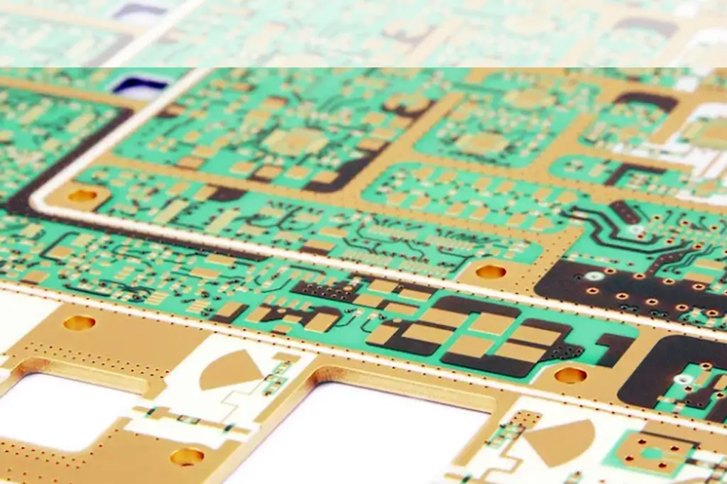
High Frequency PCB Quality Assurance
Our high frequency PCB manufacturing quality control system includes six high-frequency-exclusive tests, far exceeding the scope of standard PCB inspections:
- Temperature-Cycled Dk/Df Testing: Verify the stability of dielectric constant and loss across a -40°C to 85°C range for each substrate batch, ensuring no signal loss variation in extreme operating environments.
- Insertion Loss Measurement: Use a vector network analyzer to measure insertion loss at target frequencies (e.g., ≤0.5dB/inch at 24GHz for 5G base station boards).
- Phase Stability Validation: Confirm phase shift ≤5° at 10GHz for high frequency PCBs used in phased array radar systems, where signal synchronization is critical.
- X-Ray Via Void Inspection: Check blind/buried vias for voids, with a maximum allowable void rate of ≤0.5% to eliminate signal reflection points.
- Aerospace-Grade Thermal Cycling: Subject aerospace-grade high frequency circuit boards to 1000 cycles of -40°C to 125°C thermal shock, simulating years of in-service temperature stress.
- ESD Protection Testing: Ensure surface resistance falls within the 10⁶–10⁹Ω range to provide reliable electrostatic discharge (ESD) protection for telecom applications.
All product batches are accompanied by a comprehensive test report, suitable for regulatory submissions such as FCC certification for telecom devices and AS9100 compliance for aerospace equipment.
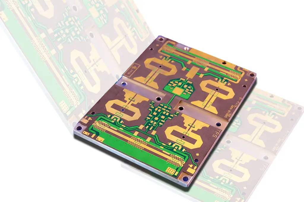
High Frequency PCB Industry Applications
5G Telecom High Frequency PCB Case
We delivered over 200,000 high frequency PCB units to a leading global 5G vendor, leveraging Rogers RO4350B material and our specialized high frequency PCB design service to achieve ±3% impedance control and ≤0.5dB/inch insertion loss at 24GHz. Compared to competitor boards, our high frequency circuit boards reduced base station signal loss by 20%, enabling the vendor to expand 5G coverage by 25% in dense urban areas with complex building layouts. All boards passed FCC certification and achieved a 99.9% first-pass yield in mass production.
Aerospace Radar High Frequency PCB Case
Our high frequency PCBs were integrated into a satellite phased array radar system, using PTFE substrates and blind/buried vias to achieve phase stability ≤5° at 35GHz. The high frequency circuit boards withstood 1000 hours of thermal cycling testing and obtained AS9100 aerospace certification. During two years of on-orbit operation testing, the boards exhibited zero performance degradation— a milestone that validated our capability to deliver high-reliability high frequency PCBs for mission-critical aerospace applications.
High Frequency PCB Capabilities
When it comes to high frequency PCB design, it’s important that the design engineer collaborate with the PCB supplier to select the materials for the desired frequency performance requirements and to establish the correct stack-up. Benchuang Electronics has deep engineering capabilities and experience with control depth drilling, control depth milling, and back drilling, unlike some of our competitors. This means we have the technology, the experience, and the knowledge to help you design and build the right high frequency PCB from the start.
High frequency PCB Design Guidelines
Download our design guidelines for high frequency PCBs
To prevent getting it wrong from the start, we have put together our design guidelines, to use as a checklist.
The file lists some of the fabrication features that are typically associated with high frequency PCB. The feature limits listed are not comprehensive; Our experienced engineers have also worked with every type of PCB material, so they have the knowledge and expertise to provide recommendations and answer all of your high frequency PCB questions. Most importantly, they know how to assist for manufacturability and the potential cost drivers of a project.
| Description | Production | Advanced |
|---|---|---|
| Inner Layer | ||
| Min.Trace/Space | 1.5mils / 1.5mils | 1.2mils / 1.5mils |
| Min. Copper Thickness | 1/3oz | 1/7 oz |
| Max. Copper Thickness | 10oz | 30oz |
| Min. Core Thickness | 2mils | 1.5mils |
| Line/ pad to drill hole | 7mils | 6mils |
| Line/ pad to board edge | 8mils | 7mils |
| Line Tolerance | +/-10% | +/-10% |
| Board Dimensions | ||
| Max. Finish Board Size | 19”X26” | 20”X28” |
| min. Finish Board Size | 0.2"X0.2" | 0.15"X0.15" |
| Max. Board Thickness | 0.300"(+/-10%) | 0.350"(+/-8%) |
| Min. Board Thickness | 0.007"(+/-10%) | 0.005"(+/-10%) |
| Lamination | ||
| Layer Count | 60L | 100L |
| Layer to Layer Registration | +/-4mils | +/-2mils |
| Drilling | ||
| Min. Drill Size | 6mils | 5mils |
| Min. Hole to Hole Pitch | 16mils(0.4mm) | 14mils(0.35mm) |
| True position Tolerance | +/-3mils | +/-2mils |
| Slot Diameter Tolerance | +/-3mils | +/-2mils |
| Min gap from PTH to track inner layers | 7mils | 6mils |
| Min. PTH edge to PTH edge space | 9mils | 8mils |
| Plating | ||
| Max. Aspect Ratio | 28:1 | 30:1 |
| Cu Thickness in Through hole | 0.8-1.5 mils | 2 oz |
| Plated hole size tolerance | +/-2mils | +/-1.5mils |
| NPTH hole tolerance | +/-2mils | +/-1mils |
| Min. Via in pad Fill hole size | 6mils | 4mils |
| Via in pad Fill Material | Epoxy resin/Copper paste | Epoxy resin/Copper paste |
| Outer Layer | ||
| Min. Trace/Space | 2mils / 2mils | 1.5mils / 1.5mils |
| Min. pad over drill size | 6mils | 5mils |
| Max. Copper thickness | 12 oz | 30 oz |
| Line/ pad to board edge | 8mils | 7mils |
| Line Tolerance | +/-15% | +/-10% |
| Metal Finish | ||
| HASL | 50-1000u” | 50-1000u” |
| HASL+Selective Hard gold | Yes | Yes |
| OSP | 8-20u” | 8-20u” |
| Selective ENIG+OSP | Yes | Yes |
| ENIG(Nickel/Gold) | 80-200u”/2-9 u” | 250u”/ 10u” |
| Immersion Silver | 6-18u” | 6-18u” |
| Hard Gold for Tab | 10-80u” | 10-80u” |
| Immersion Tin | 30u”min. | 30u” min. |
| ENEPIG (Ni/Pd/Au) | 125u"/4u"/1u” min. | 150u"/8u"/2u” min. |
| Soft Gold (Nickel/ Gold) | 200u”/ 20u”min. | 200u”/ 20u” |
| Solder Mask | ||
| S/M Thickness | 0.4mils min. | 2mils max. |
| Solder dam width | 4mils | 3mils |
| S/M registration tolerance | +/-2mils | +/-1.5mils |
| S/M over line | 3.5mils | 2mils / 2mils |
| Legend | ||
| Min. Space to SMD pad | 6mils | 5mils |
| Min. Stroke Width | 6mils | 5mils |
| Min. Space to Copper pad | 6mils | 5mils |
| Standard Color | White , Yellow, Black | N/A |
| Electrical Testing | ||
| Max. Test Points | 30000 Points | 30000 Points |
| Smallest SMT Pitch | 16mils(0.4mm) | 12mils(0.3mm) |
| Smallest BGA Pitch | 10mils(0.25mm) | 6mils(0.15mm) |
| NC Rout | ||
| Min. Rout to copper space | 8mils | 7mils |
| Rout tolerance | +/-4mils | +/-3mils |
| Scoring (V-cut) | ||
| Conductor to center line | 15mils | 15mils |
| X&Y Position Tolerance | +/-4mils | +/-3mils |
| Score Anger | 30o/45o | 30o/45o |
| Score Web | 10mils min. | 8mils min. |
| Beveling | ||
| bevel anger | 20-71o | 20-71o |
| Bevel Dimensional Tolerance | +/-10mils | +/-10mils |
| Impedance controll | ||
| Impedance controll | +/-10% | +/-7% |
View More +
High Frequency PCB Materials
Special materials are required to achieve the high frequency provided by this type of PCB. There are a variety of substrate materials that will support your design and may differ based on signal speeds required and the application/environment of the circuit board.
In terms of price, FR4 is the least expensive compared to dedicated high speed materials and Teflon, with Teflon being the most expensive. Though, FR-4 starts to drop off in performance when signal speed edges above 1.6ghz
Newer generation substrates, Teflon, and flex circuits are the best options when it comes to Dk, Df, water absorption, and survivability in the environment
If a printed circuit board requires a frequency above 10GHz, newer generation substrates, Teflon, and Flex substrates are your best option since they are far superior to traditional FR-4 material.
The most common suppliers of high speed substrates are Rogers, Isola, Taconic and Megtron materials by Panasonic. All of these materials typically are lower Dk and lower loss.
High Frequency PCB Material Properties
There are a few material properties that should receive focus when shopping for high frequency PCB materials. There are multiple vendors that produce these materials, and they all try to compete with each other based on the electromagnetic properties for the materials they produce. You can spot all of the material properties I’ll specify below in the datasheest provided by the vendor.
Dk and Df (Loss Tangent)
This is probably the most common point everyone will start looking for when they dive into datasheets. Material vendors will report these values at specific frequencies, usually 1 GHz or 10 GHz, depending on the target market for the material. I think most designers will start looking for this specification because they will be operating with a system that needs to have low loss, so they will generally start by comparing dielectric loss values.
The important factor to focus on depends on the type of high frequency PCB you want to design:
- If your target is to make very small RF printed circuits, then you need a larger real part of the dielectric constant.
- If your target is low loss, then you should aim for low imaginary part of the dielectric constant..
If your interconnects will be very long and there is a risk of excessive losses, then you should use a material with a smaller imaginary part of the dielectric constant. The real part (Dk) has nothing to do with dielectric losses when the impedance is fixed at your target value. However, Dk does matter because it determines the wavelength of your operating signal in your high frequency PCB. Smaller circuits generally need a smaller wavelength, which means you will need a larger Dk value.
One important point that arises in any RF printed circuit that relies on resonance (such as waveguides, antennas, and resonators) is the direction of the electric field. The dielectric constant of substrate materials will be different along each axis in the material, therefore the dielectric constant that will determine wave propagation speed and resonance will depend on the direction of the electric field in the system. These differences might only be about 5%, but they matter in some high-Q structures like short resonators and emitters that support modulated signals. The dielectric constant value corresponding to different electric polarization directions should be specified in your material datasheets.
Available Thickness and Panel Size
- Use a larger Dk value to get smaller circuits
- Use a thinner laminate to get smaller circuits
| Typical Thicknesses1 | |
|---|---|
| Inches | mm |
| 0.010 | 0.25 |
| 0.020 | 0.51 |
| 0.030 | 0.76 |
| 0.060 | 1.52 |
| Typical Panel Sizes2 | |
|---|---|
| Inches | mm |
| 12 x 18 | 205 x 457 |
| 16 x 18 | 406 x 457 |
| 18 x 24 | 457 x 610 |
| 36 x 48 | 914 x 1220 |
Typical materials used for high-frequency boards?
The following materials are suitable for a high-frequency PCB manufacturing process:
- Materials, namely, Isola I-speed, Isola Astra, and Tachyon exhibit low loss at high frequencies.
- Rogers 4350B and Panasonic Megtron 6
- Rogers 4350B show cases low loss and is suitable in the frequency range of 500MHz to 3GHz.
- Panasonic Megtron 6 also show cases low loss and is suitable in the frequency range of 3GHz and above.
Simply put, it is a multilayer printed circuit board designed to carry signals from point to point at a specified frequency and speed. The signals are typically impedance controlled and on specific layers throughout the high-performance printed circuit board.
PCBs are usually produced on specialty laminate materials such as Rogers, Taconic, Isola, or Arlon to name a few. The board can be rigid, flex, or a combined rigid-flex and come in many different sizes, shapes, and thicknesses.
Material selection, layer stack-up, trace width and spacing, via placement, grounding, and signal integrity analysis are critical factors that should be considered while designing high-frequency PCBs. These PCBs are a type of electronic substrate that is designed to handle high-frequency signals. They are used in a variety of applications such as communication systems, radar systems, and medical equipment. Proper design of these PCBs will result in better signal quality and improved system performance.
High Frequency PCB Design Tips
- Material Selection
- Layer Stack-up
- Trace Width & Spacing
- Via Placement
- Grounding
- Signal Integrity
When you are designing printed circuit boards for your application, it is important to use materials that are going to give you the performance you need to make it a success. If you need something specifically for a high frequency, microwave or RF application, you will need to work with a manufacturer to get the laminates that will keep everything on track.
These laminates often require different types of b-stage/prepreg or bonding sheets to laminate them for multilayer PCB designs. The most commonly used is the Rogers RO4000 series. Talk with an expert at Benchuang Electronics to learn about the materials that are best for your PCBs.
Since then we have kept improving our experience of different base materials – and today we can process many different materials and even mixed buildups.
High frequency PCBs are typically used in radio and high speed digital applications such as 5G or 6G wireless communication, automotive radar sensors, aerospace, satellites and more. High frequency laminates provide lower attenuation and constant dielectric properties compared to PCBs of conventional FR4 materials. Benchuang Electronics has specialized in the manufacture of multilayer and HDI PCBs of high frequency dielectric materials.
Get started with High Frequency PCB
- Blind vias, buried vias, Ultra HDI PCB
- High frequency low loss PCB material
- TLY-5, RF35, RF-35TC, TSM-DS3, TLX-8, TLX-9 material
- RO4003, RO4350B, RO4835, RT/duroid 5870, RT/duroid 5880, RT/duroid 6002, TMM3, TMM4, TMM6, TMM10, TMM10i material