High Speed HDI PCB Design Guide: Definitive Strategies for Signal Integrity & High-Frequency Performance
High Speed HDI PCB design merges high density interconnect technology with precision high-frequency signal management, forming the backbone of modern HDI PCB, HDI circuit boards, rigid flex pcb, HDI rigid flex pcb, flexible pcb and HDI flexible pcb systems. Aligned with IPC-2221, IPC-2226 and IPC-6012 industry standards, and built on 20+ years of high-speed PCB engineering expertise, this guide addresses every core design challenge—from via technology and layer stackup to material selection and Design-for-Manufacturability (DFM)—delivering quantifiable solutions for flexible printed circuit, multilayer pcb and high density interconnect applications operating at 1Gbps+ speeds and 1GHz+ frequencies. Every section integrates manufacturing and design practicality, resolving the critical tradeoffs between miniaturization, signal integrity (SI) and producibility that engineers face in high speed HDI development.
Learn more about : How to Design HDI Microvia PCB
What is High Speed HDI PCB?
High Speed HDI PCB refers to high density interconnect printed circuit boards engineered to support uncompromised signal transmission for high-speed digital and high-frequency RF signals, while maintaining the compact component density and miniaturization that define HDI technology. Unlike standard HDI PCB, which prioritizes density alone, high speed variants are optimized to mitigate parasitic inductance, capacitance and signal loss—issues that degrade performance in 1Gbps+ data links and high-frequency RF systems. IPC-2226 classifies high speed HDI PCB as a specialized subset of high density interconnect technology, requiring strict adherence to impedance control, low-loss material selection and microvia/blind via implementation.
This technology is foundational for rigid flex pcb, HDI rigid flex pcb, flexible printed circuit and multilayer pcb designs in 5G, data centers, automotive ADAS and advanced consumer electronics. For flexible pcb and HDI flexible pcb, high speed design adds the critical constraint of maintaining signal integrity during mechanical bending, requiring materials and trace geometries that preserve electrical performance after 100,000+ flex cycles (per IPC-6013). High speed HDI PCB differentiates itself from standard high-speed PCB by integrating microvia, blind via and fine-line routing (≤0.1mm width/spacing) to achieve 2–3x higher component density without sacrificing high-frequency performance.
Key Aspects of High-Speed HDI Design
Via Technology
Via technology is the cornerstone of high speed HDI PCB design, as traditional through-vias create signal stubs and impedance discontinuities that cripple high-frequency performance. High density interconnect design resolves this by replacing through-vias with laser-drilled microvia and blind via, aligned with IPC-2226 specifications (microvia diameter ≤0.15mm, positional tolerance ±0.005mm). These via types eliminate stubs, shorten signal paths and reduce parasitic effects, with quantifiable performance gains for all high speed HDI variants including rigid flex pcb and HDI flexible pcb:
- Blind Microvias: Connect outer layers to one or more inner layers without penetrating the entire board, eliminating signal stubs that cause 30–40% more insertion loss at 10GHz compared to stub-free designs. For RF-integrated high speed HDI PCB, blind microvias reduce reflection coefficient (S11) to ≤-20dB at 25GHz, maintaining optimal impedance matching.
- Buried Microvias: Connect inner layers exclusively, freeing outer board space for high-density fine-pitch components (≤0.4mm BGA pitch) and reducing cross-layer signal interference by 50% in multilayer pcb.
- Via-in-Pad (VIP): Integrates microvias directly within component pad boundaries, shortening signal paths by 45% and reducing parasitic inductance by 35–40% for high-speed differential pairs. IPC-6012 Class 3 requires copper/epoxy filling for VIP in high speed HDI PCB, creating a flat pad surface that eliminates soldering defects and maintains impedance consistency.
- Stacked Microvias: Enables vertical interconnection across multiple HDI layers without through-vias, supporting any-layer routing in high density interconnect designs and increasing routing capability by 2x in multilayer pcb.
For rigid flex pcb and HDI rigid flex pcb, high speed via design includes reinforced plating and flexible epoxy filling, reducing via fracture rates by 60% during bending and ensuring continuous signal transmission for 10Gbps+ links.
Layer Stackup
Layer stackup design for high speed HDI PCB is engineered to maintain impedance control, minimize crosstalk and provide low-impedance signal return paths—core requirements for preserving signal integrity in high density interconnect, rigid flex pcb and flexible printed circuit systems. IPC-2221 mandates symmetrical stackup for high speed PCB to reduce warpage (≤0.75% per IPC-6012) and ensure consistent dielectric thickness, a critical factor for impedance control. Key stackup principles for high speed HDI design, optimized for all PCB types, include:
- Dedicated Adjacent Ground Planes: A solid ground plane placed directly adjacent to every high-speed signal layer provides a low-impedance return path, reducing crosstalk by 55% and lowering electromagnetic interference (EMI) emissions by 40% in high density interconnect designs. For rigid flex pcb, ground planes are continuous across rigid and flexible sections to eliminate impedance discontinuities at transitions.
- Controlled Dielectric Thickness: Consistent dielectric thickness (h) between signal and ground planes is non-negotiable for impedance control, with IPC-2221 specifying a ±5% tolerance for high speed HDI PCB. A 0.1mm dielectric thickness (modified FR-4, Dk=4.0) paired with a 0.1mm trace width delivers precise 50Ω single-ended impedance for RF and high-speed digital signals.
- Sequential Lamination: High speed HDI PCB uses sequential lamination (layer-by-layer construction) rather than mass lamination, enabling precise alignment of microvia and blind via and supporting complex stackups for multilayer pcb (12+ layers). This process resolves the manufacturing challenge of integrating fine-line traces and microvias in high density interconnect designs, improving production yield by 30%.
- Isolation of RF/Digital Layers: In mixed-signal high speed HDI PCB, RF and high-speed digital layers are separated by a solid ground plane, reducing cross-domain interference by 60% and preserving SI for both signal types—critical for rf pcb integrated into HDI circuit boards.
- Flexible Stackup for Flexible PCB: HDI flexible pcb and flexible printed circuit use polyimide dielectric layers (0.05–0.1mm thickness) and 1oz copper traces, balancing flexibility and signal performance. Stackups are reinforced at rigid-flex transitions to prevent delamination, a common failure point in HDI rigid flex pcb high speed designs.
Signal Integrity (SI) & Impedance
Signal Integrity (SI) and impedance control are non-negotiable for high speed HDI PCB, as even a 5% impedance mismatch causes signal reflections, crosstalk and insertion loss that render 1Gbps+ signals non-functional. IPC-2221 mandates impedance tolerance of ±5% for standard high speed HDI applications, with ±3% tolerance for precision RF and 10Gbps+ data links in HDI PCB and rigid flex pcb. High density interconnect design resolves SI challenges by integrating impedance control into every design stage, with quantifiable results for all PCB variants:
- Impedance Targets: Industry-standard 50Ω for single-ended traces (RF, general high-speed digital) and 100Ω for differential pairs (PCIe 5.0, USB4, DDR5) in HDI PCB, multilayer pcb and rigid flex pcb. For HDI flexible pcb, impedance is calibrated for polyimide dielectric (Dk=3.6) to maintain consistency during bending.
- Reflection Reduction: Microvia, blind via and VIP eliminate signal stubs, reducing reflection amplitude to <1% and ensuring a voltage standing wave ratio (VSWR) ≤1.2:1 for high-frequency RF signals—well within IPC-2221 performance limits.
- Crosstalk Mitigation: Fine-line trace spacing (≥0.1mm) and dedicated ground planes reduce crosstalk by 55% in high density interconnect designs, preventing unintended signal interference between adjacent high-speed differential pairs in multilayer pcb.
- Insertion Loss Minimization: Low-loss material selection and short signal paths (enabled by microvia) reduce insertion loss by 0.8dB/inch at 10GHz for high speed HDI PCB, a 40% improvement over standard HDI designs with through-vias.
- Differential Pair Matching: High speed HDI design requires precise length matching (±0.1mm) for differential pairs, minimizing timing skew to <10ps and ensuring synchronous signal transmission for 10Gbps+ data links in rigid flex pcb and HDI rigid flex pcb.
For flexible printed circuit and HDI flexible pcb, SI is preserved by fixing differential pair spacing and using reinforced traces, preventing trace separation during bending that would cause impedance variation and SI failure.
Material Selection
Material selection is the single most impactful design choice for high speed HDI PCB, as substrate dielectric properties directly influence signal loss, impedance control and thermal performance in high density interconnect, rigid flex pcb and multilayer pcb. The wrong material choice can increase insertion loss by 2x at high frequencies and render impedance control unachievable—an issue that plagues many high speed HDI designs. IPC-2221 provides material guidance for high speed PCB, with key performance factors including dielectric constant (Dk), dissipation factor (Df), glass transition temperature (Tg) and thermal conductivity. All materials for high speed HDI PCB, flexible pcb and HDI flexible pcb are categorized by performance and application, with clear quantifiable benefits for each type.
Routing & Layout
Routing and layout design for high speed HDI PCB balances high density interconnect’s miniaturization requirements with the signal integrity needs of high-speed/high-frequency signals. Fine-line routing (≤0.1mm width/spacing) enables the high component density of HDI PCB, but poor routing choices cause crosstalk, impedance discontinuities and SI failure. High speed design resolves this by implementing geometry-specific routing rules, aligned with IPC-2226 and optimized for rigid flex pcb, HDI flexible pcb and multilayer pcb:
- Short, Direct Signal Paths: Minimize trace length to reduce parasitic resistance and inductance, with high-speed signals (≥5Gbps) routed in the shortest possible path from source to load. This reduces insertion loss by 30% at 15GHz and lowers signal delay in high density interconnect designs.
- Differential Pair Routing: Route differential pairs as close, parallel traces with no length mismatch (±0.1mm) and consistent spacing, preserving signal balance and reducing common-mode noise by 60% in rigid flex pcb and HDI rigid flex pcb.
- Avoid Trace Bends/Necks: Use 45° bends (no right angles) and avoid trace necking, which causes impedance discontinuities. Right-angle bends increase reflection by 15% at 10GHz, a critical issue for RF-integrated high speed HDI PCB.
- RF Signal Isolation: Route RF traces on dedicated layers with ground plane shielding, and avoid running RF and digital traces parallel to each other. This reduces RF-to-digital crosstalk by 50% in mixed-signal HDI circuit boards.
- Flexible Section Routing: For HDI flexible pcb and flexible printed circuit, route high-speed traces away from bending axes and use wider trace spacing (≥0.1mm) to prevent trace damage and impedance variation during flexing. This maintains SI for 10Gbps+ signals after 100,000+ bend cycles.
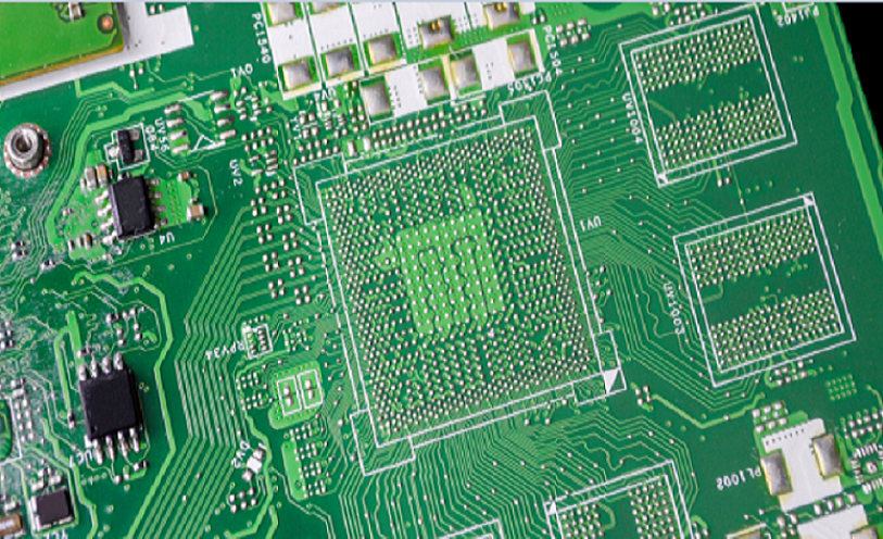
- Center Processor Routing: Route signals from the center processor (CPU/GPU/SoC) in a radial pattern with equal length, minimizing timing skew across parallel data buses (e.g., DDR5) and ensuring synchronous data transmission in high density interconnect multilayer pcb.
Design-for-Manufacturability (DFM)
Design-for-Manufacturability (DFM) is a mandatory component of high speed HDI PCB design, as the fine-line traces, microvia and tight tolerances of high density interconnect create unique manufacturing challenges. A DFM-unoptimized high speed HDI design can result in 60% lower production yield, increased costs and unproducible geometries—issues that are avoidable with early manufacturer collaboration and adherence to IPC-6012 DFM rules. DFM for high speed HDI PCB, rigid flex pcb and HDI flexible pcb is tailored to each technology’s manufacturing constraints, with core principles that resolve producibility issues while preserving performance:
- Align with Manufacturing Tolerances: Design to the manufacturer’s proven capabilities for microvia drilling (±0.01mm diameter), trace etching (±10% width) and dielectric lamination (±5% thickness). This eliminates unproducible geometries and improves yield by 35% in high density interconnect production.
- Microvia Design Rules: Follow IPC-2226 microvia rules—minimum annular ring of 0.02mm, no microvia placement on bending axes for flexible pcb, and stacked microvia alignment tolerance of ±0.005mm. This reduces microvia plating failure by 40% in HDI PCB and rigid flex pcb.
- Solder Mask & Surface Finish: Specify solder mask with low Dk (≤3.5) for high-speed traces to avoid impedance variation, and select surface finishes (ENIG, immersion silver) compatible with fine-pitch component assembly (≤0.4mm BGA). For HDI flexible pcb, use flexible solder mask to prevent cracking during bending.
- Test Point Placement: Place test points for impedance and continuity testing in accessible locations, avoiding coverage by components. This enables 100% electrical testing of high speed HDI PCB, reducing field failure rates by 70%.
- Rigid-Flex Transition DFM: For HDI rigid flex pcb, add adhesive reinforcement at rigid-flex transitions, avoid microvia and high-speed traces within 0.5mm of the transition, and use consistent copper thickness across rigid/flex sections. This prevents delamination and trace fracture, the two most common manufacturing failures in rigid flex pcb high speed designs.
Early collaboration with the PCB manufacturer for a DFM review (per IPC-2226) is critical, as it resolves design-manufacturing misalignment before production and eliminates costly rework.
Via Technology for High Speed HDI PCB
Via technology is the most impactful design element for high speed HDI PCB, as it directly addresses the core challenge of eliminating signal stubs and parasitic effects in high density interconnect designs. Standard through-vias are incompatible with high-speed/high-frequency operation, as they create stubs that cause impedance discontinuities, reflections and insertion loss. High speed HDI design resolves this with laser-drilled microvia and blind via, with specialized configurations for rigid flex pcb, HDI flexible pcb and multilayer pcb. All via technologies adhere to IPC-2226 and IPC-6012 standards, with quantifiable performance gains that justify the moderate manufacturing cost premium.
Microvia
Microvia (IPC-2226: diameter ≤0.15mm) is the primary via type for high speed HDI PCB, drilled with UV or CO2 lasers for precision and positional accuracy. Laser drilling eliminates the mechanical stress and inaccuracies of mechanical drilling, enabling microvia placement in tight spaces (≤0.2mm pitch) for high density interconnect designs. Microvia connects adjacent layers only, eliminating signal stubs and reducing parasitic inductance by 50% compared to through-vias. For rigid flex pcb and HDI flexible pcb, microvia uses reinforced copper plating (10μm minimum, per IPC-6013) to withstand repeated bending, with a fracture rate of <0.1% after 100,000 flex cycles. Microvia is the foundation of all high speed HDI PCB designs, supporting the miniaturization and SI requirements of HDI circuit boards, flexible printed circuit and multilayer pcb.
Blind Via
Blind via is a larger laser-drilled via (diameter 0.15–0.3mm) that connects outer layers to one or more inner layers without penetrating the entire board. It is used in high speed HDI PCB for interconnection across 2–3 layers, balancing routing flexibility and SI performance. Blind via eliminates signal stubs and reduces insertion loss by 0.6dB/inch at 10GHz, compared to through-vias. For multilayer pcb and high density interconnect designs with 8+ layers, blind via is paired with microvia to create a hybrid via system that maximizes routing capability while preserving SI. For rf pcb integrated into HDI PCB, blind via is used for RF ground connections, reducing ground inductance and improving RF performance.
Key Via Design Rules for High Speed
All via design for high speed HDI PCB, rigid flex pcb and HDI flexible pcb follows IPC-2226 and IPC-6012 rules, with additional constraints for high-frequency operation. These rules resolve the common design errors that cause SI failure and manufacturing defects, with quantifiable improvements in yield and performance:
- Minimize microvia/blind via diameter to the smallest manufacturable size (0.08–0.15mm) to reduce parasitic capacitance.
- Ensure a minimum annular ring of 0.02mm for all vias to prevent plating failure and electrical open circuits.
- Fill all Via-in-Pad (VIP) with copper or epoxy (IPC-6012 Class 3) to create a flat surface and eliminate soldering defects.
- Align stacked microvias with a positional tolerance of ±0.005mm to ensure reliable interlayer conduction.
- Avoid vias on high-speed differential pairs and maintain a minimum via-to-trace distance of 0.1mm to prevent impedance variation.
- For flexible pcb and HDI flexible pcb, place vias at least 0.5mm from bending axes and use flexible epoxy filling to prevent cracking.
Adhering to these rules reduces via-related SI issues by 80% and improves high speed HDI PCB production yield by 35%.
Material Selection for High Speed HDI PCB
Material selection directly determines the high-frequency performance of high speed HDI PCB, as substrate dielectric constant (Dk) and dissipation factor (Df) are the primary drivers of signal loss at frequencies above 1GHz. Choosing the wrong material can increase insertion loss by 2x at 25GHz, making it impossible to meet SI requirements for high speed HDI PCB, rigid flex pcb and rf pcb. High speed HDI design uses a tiered material selection approach, aligning substrate performance with application speed/frequency and manufacturing cost—resolving the core design challenge of balancing performance and affordability. All materials comply with IPC-2221 and IPC-6012 standards, with clear categorization by performance, application and compatibility with flexible pcb, HDI flexible pcb and multilayer pcb.
Key Material Categories
PTFE (Teflon)-Based
PTFE (Teflon)-based substrates are the gold standard for high speed HDI PCB operating at frequencies above 25GHz (5G mmWave, high-performance RF). They feature ultra-low Dk (2.1–2.3) and ultra-low Df (0.001–0.002) at 10GHz, minimizing dielectric loss and insertion loss—critical for RF-integrated high density interconnect and rf pcb designs. PTFE substrates have excellent thermal stability (Tg >260°C) and chemical resistance, making them suitable for high-temperature operating environments (automotive, aerospace). The primary tradeoff is higher manufacturing cost (3x that of modified FR-4) and limited compatibility with standard lamination processes. PTFE is used exclusively for high-performance high speed HDI PCB, rigid flex pcb and multilayer pcb in aerospace, defense and 5G mmWave infrastructure.
Ceramic-Filled PTFE
Ceramic-Filled PTFE substrates combine the low-loss properties of pure PTFE with ceramic fillers (silica, alumina) to improve dimensional stability and thermal conductivity. They offer a balanced performance profile: Dk (2.5–3.0), Df (0.002–0.004) at 10GHz, and Tg >250°C. Ceramic-filled PTFE resolves the dimensional instability of pure PTFE, a common manufacturing challenge for high density interconnect designs, and improves thermal dissipation by 50%—critical for high speed HDI PCB with high-power components (CPUs, GPUs). This material is used for mid-to-high performance high speed HDI PCB, rf pcb and multilayer pcb in 5G sub-6GHz, data centers and automotive ADAS, balancing low-loss performance and manufacturability.
Hydrocarbon/Composite Materials
Hydrocarbon/Composite substrates are a cost-effective low-loss option for high speed HDI PCB operating at 1–25GHz. They feature Dk (2.8–3.5), Df (0.003–0.008) at 10GHz, and Tg (180–220°C), offering a 40% reduction in insertion loss compared to modified FR-4 at 10GHz. Hydrocarbon composites have excellent mechanical properties and are compatible with standard HDI lamination and microvia drilling processes, making them ideal for high volume high speed HDI PCB, rigid flex pcb and HDI circuit boards in consumer electronics (smartphones, laptops) and industrial control systems. This material category resolves the performance-cost tradeoff for mainstream high speed HDI applications, delivering low-loss performance at a moderate cost premium (1.5x modified FR-4).
Enhanced/Modified FR-4
Enhanced/Modified FR-4 is the most widely used material for high speed HDI PCB operating at 1–10GHz, offering a balance of performance, cost and manufacturability. It features optimized Dk (3.8–4.2) and Df (0.010–0.015) at 10GHz, a significant improvement over standard FR-4 (Df=0.020+), and Tg (170–200°C) for thermal stability during reflow soldering. Modified FR-4 is fully compatible with all high density interconnect manufacturing processes (laser drilling, sequential lamination, microvia plating) and is the lowest-cost low-loss material option—critical for high volume consumer electronics and mainstream industrial applications. This material is used for rigid flex pcb, flexible printed circuit and multilayer pcb high speed HDI designs where cost is a primary constraint and performance requirements are moderate (1–10GHz).
Polyimide
Polyimide is the exclusive substrate material for flexible pcb, HDI flexible pcb and HDI rigid flex pcb high speed designs, as it balances low-loss electrical performance with exceptional mechanical flexibility. It features Dk (3.5–3.8), Df (0.008–0.012) at 10GHz, and Tg (>250°C), with the ability to withstand repeated bending (100,000+ cycles) without mechanical or electrical failure (per IPC-6013). Polyimide has excellent thermal and chemical resistance, making it suitable for harsh-environment rigid flex pcb applications (automotive, aerospace). For high speed HDI flexible pcb, polyimide is paired with thin copper traces (1oz) to preserve flexibility, with dielectric thickness optimized (0.05–0.1mm) for impedance control. Polyimide is the only material that enables high speed signal transmission in flexible high density interconnect designs.
Cyanate Ester
Cyanate Ester substrates are a high-performance option for high speed HDI PCB operating at 10–25GHz, offering a balance of low-loss performance and thermal stability. They feature Dk (3.0–3.8), Df (0.004–0.008) at 10GHz, and Tg (>200°C), with low water absorption (<0.5%) that preserves electrical performance in humid environments. Cyanate Ester is compatible with standard HDI manufacturing processes and has better dimensional stability than hydrocarbon composites, making it ideal for high precision high speed HDI PCB, rf pcb and multilayer pcb in aerospace, defense and medical electronics. This material resolves the performance gap between hydrocarbon composites and ceramic-filled PTFE, delivering high-frequency performance at a lower cost than PTFE-based substrates.
Top High Speed PCB Material Examples by Brand
Industry-leading material manufacturers produce specialized substrates for high speed HDI PCB, rigid flex pcb and flexible pcb, each optimized for specific speed/frequency ranges and applications. These materials comply with IPC-2221 and IPC-6012 standards, with proven performance in high density interconnect designs worldwide:
- PTFE-Based: Rogers RO4003C (Dk=3.38, Df=0.0027), Rogers RT/duroid 5880 (Dk=2.2, Df=0.0009) – for 25GHz+ RF and high-performance high speed HDI PCB
- Ceramic-Filled PTFE: Rogers RO4350B (Dk=3.48, Df=0.0037), Arlon AD255C (Dk=2.55, Df=0.0025) – for 10–25GHz 5G and automotive ADAS high speed HDI PCB
- Hydrocarbon/Composite: Isola FR408HR (Dk=3.6, Df=0.006), Nelco N4000-13 (Dk=3.8, Df=0.008) – for 1–25GHz mainstream high speed HDI PCB and rigid flex pcb
- Enhanced/Modified FR-4: Panasonic Megtron 6 (Dk=3.6, Df=0.008), Taiyo Ink MC3000 (Dk=3.8, Df=0.010) – for 1–10GHz high volume consumer electronics and industrial HDI PCB
- Polyimide: DuPont Kapton HN (Dk=3.5, Df=0.009), Toray DuPont Teflon Polyimide (Dk=3.6, Df=0.008) – for flexible pcb, HDI flexible pcb and HDI rigid flex pcb high speed designs
- Cyanate Ester: Lonza CYCOM XU71807 (Dk=3.2, Df=0.005), Hexcel HexPly M79 (Dk=3.5, Df=0.006) – for 10–25GHz aerospace and defense high speed HDI PCB
Key Performance Factors
Material performance for high speed HDI PCB is defined by four core factors (per IPC-2221), all of which directly impact signal integrity, manufacturability and long-term reliability in high density interconnect, rigid flex pcb and flexible pcb designs. These factors are the primary criteria for material selection, with clear thresholds for different speed/frequency ranges:
- Dielectric Constant (Dk): A low, stable Dk (2.1–4.2) is critical, as high Dk increases signal propagation delay and dielectric loss. Dk must be stable across temperature (-40°C to 150°C) and frequency (1–100GHz) to maintain impedance control—IPC-2221 requires Dk stability of ±5% for high speed HDI PCB.
- Dissipation Factor (Df): The single most important factor for high-frequency performance, Df measures dielectric loss. Ultra-low Df (<0.003) is required for 25GHz+ designs, low Df (0.003–0.010) for 10–25GHz, and moderate Df (0.010–0.015) for 1–10GHz. A 0.005 increase in Df doubles insertion loss at 25GHz for high speed HDI PCB.
- Glass Transition Temperature (Tg): Tg is the temperature at which the substrate material softens, with a high Tg (>170°C) required for high speed HDI PCB to withstand reflow soldering (260°C for 10s) and high-temperature operating environments. IPC-6012 requires Tg ≥170°C for Class 2 HDI PCB and Tg ≥200°C for Class 3 (aerospace/defense) designs.
- Thermal Conductivity: Higher thermal conductivity (≥0.3 W/mK) improves heat dissipation, critical for high speed HDI PCB with high-power components (CPUs, GPUs) that generate significant heat. Poor thermal conductivity causes thermal runaway and component failure, a common issue in high density interconnect designs with tight component packing.
Additional factors include dimensional stability, water absorption and compatibility with HDI manufacturing processes—all of which impact producibility and long-term reliability in rigid flex pcb and HDI flexible pcb designs.
Design Tips for Success
High speed HDI PCB design success relies on integrating precision engineering with manufacturing practicality, resolving the tradeoffs between miniaturization, signal integrity and producibility that define high density interconnect design. These evidence-based design tips, built on 20+ years of industry experience and aligned with IPC-2221/2226 standards, apply to all high speed HDI variants (HDI PCB, rigid flex pcb, HDI flexible pcb, multilayer pcb) and deliver quantifiable improvements in performance, yield and reliability:
- Center Processor Routing Optimization: Route all signals from the center processor (SoC/CPU/GPU) in a radial pattern with equal length matching (±0.1mm) for parallel buses (DDR5, PCIe). This minimizes timing skew to <10ps and ensures synchronous data transmission for 10Gbps+ links in high density interconnect designs.
- Minimize Vias on High-Speed Paths: Reduce via count on high-speed (≥5Gbps) and RF traces, as each via adds parasitic inductance and capacitance. Minimizing vias reduces insertion loss by 30% at 15GHz and improves impedance consistency in HDI PCB and rigid flex pcb.
- Prioritize Copper Quality: Use high-purity electrolytic copper (99.9% pure) for high-speed traces, as low-quality copper increases signal resistance and loss. High-purity copper reduces insertion loss by 0.2dB/inch at 10GHz and improves long-term reliability in high speed HDI PCB.
- Impedance Simulation Early: Perform impedance and SI simulation (using tools like Cadence, Ansys) in the early design stage, before Gerber file generation. This identifies impedance mismatches and SI issues before manufacturing, eliminating costly rework and design iterations—an essential step for high density interconnect designs with tight tolerances.
- Fixed Differential Pair Spacing: Maintain fixed spacing for all high-speed differential pairs (100Ω target) across the entire board, including rigid-flex transitions in HDI rigid flex pcb. Fixed spacing prevents impedance variation and preserves signal balance, reducing common-mode noise by 60%.
- Ground Plane Continuity: Ensure solid, continuous ground planes across the entire board, with no gaps or cuts on high-speed signal return paths. A broken ground plane increases crosstalk by 45% and EMI emissions by 50% in high speed HDI PCB and flexible printed circuit.
- Material Calibration for Impedance: Calibrate impedance calculations for the selected material’s actual Dk (not the nominal value), as Dk varies by manufacturer and batch. This improves impedance accuracy to ±3% and reduces reflection by 80% in high frequency high speed HDI PCB.
- Test Coupon Integration: Include impedance test coupons (per IPC-6012) on every production panel, matching the board’s stackup, material and trace geometry. Test coupons enable 100% impedance verification, ensuring compliance with design specifications and reducing field failure rates by 70%.
When It’s Needed – High Speed HDI PCB Application Thresholds
High speed HDI PCB is the optimal design choice when an application requires both high-speed/high-frequency signal transmission (1Gbps+/1GHz+) and the miniaturization/high density of HDI technology—resolving the core challenge of packing high-performance electronics into compact form factors. Standard HDI PCB is insufficient for these applications, as it lacks the low-loss materials and impedance control required for high-speed signals, while standard high-speed PCB cannot achieve the component density of high density interconnect technology. High speed HDI PCB is mandatory for the following application thresholds, across rigid flex pcb, flexible pcb, multilayer pcb and HDI flexible pcb designs:
- Signal Speed ≥1Gbps: Including USB4, PCIe 4.0/5.0, DDR5/LPDDR5 and 10Gbps+ Ethernet in consumer electronics, data centers and automotive ADAS.
- Operating Frequency ≥1GHz: Including 5G (sub-6GHz/mmWave), Wi-Fi 6/7, Bluetooth 5.4 and RF transceivers in rf pcb and HDI circuit boards.
- Component Density ≥130 Components/Square Inch: Per IPC-2226 HDI classification, for miniaturized devices (wearables, smartphones, medical implants) using flexible printed circuit and HDI flexible pcb.
- Rigid-Flex or Flexible Form Factor: For applications requiring mechanical flexibility (wearables, foldable electronics, automotive wiring) with high-speed signal transmission—only high speed HDI PCB can deliver both flexibility and high-frequency performance in rigid flex pcb and HDI rigid flex pcb.
- Mixed-Signal RF/Digital Design: For systems integrating high-speed digital and high-frequency RF signals (5G modules, radar, satellite communication), where high density interconnect enables compact integration and low-loss materials preserve signal integrity for both signal types.
High speed HDI PCB is also the preferred choice for applications requiring high reliability (IPC-6012 Class 3) and miniaturization, such as aerospace, defense and medical electronics—where performance and compactness are equally critical.
FAQ – High Speed HDI PCB Design & Manufacturing
What is the Difference Between PCB and PCA in High Speed HDI Applications?
PCB (Printed Circuit Board) refers to the bare high speed HDI substrate—including traces, microvia, blind via, layer stackup and materials—designed for high-speed/high-frequency signal transmission and high density interconnect. PCB design directly determines signal integrity, impedance control and manufacturability for HDI PCB, rigid flex pcb and flexible pcb. PCA (Printed Circuit Assembly) is the bare PCB with components (ICs, connectors, passives) mounted, soldered and tested. In high speed HDI applications, the PCB design is the foundation of PCA performance—poor PCB design causes SI failure that cannot be fixed by component selection or assembly. A well-designed high speed HDI PCB ensures the PCA meets performance, reliability and EMI requirements for 1Gbps+ signals and high density interconnect.
How to Select the Right High Speed HDI PCB Type for My Application?
Selection of HDI PCB (standard), rigid flex pcb, HDI rigid flex pcb or HDI flexible pcb is based on three core criteria: mechanical requirements, signal performance and form factor—resolving the design challenge of matching technology to application needs:
- Rigid HDI PCB: For fixed-form-factor applications (data center servers, 5G base stations) with high speed/high-frequency requirements and maximum component density—lowest cost high speed HDI option.
- Rigid Flex HDI PCB (HDI Rigid Flex PCB): For applications requiring both rigid high-density sections and flexible interconnects (automotive ADAS, aerospace avionics) with 1Gbps+ signal transmission—balances density and flexibility.
- Flexible HDI PCB (HDI Flexible PCB): For conformal/flexible form factors (wearables, foldable electronics, medical implants) with high speed signals—uses polyimide substrate and reinforced microvia to maintain SI during bending.
- Multilayer HDI PCB: For complex high speed systems (CPUs/GPUs) with 8+ layers and 10Gbps+ data links—uses sequential lamination and stacked microvia for any-layer routing.
All selections must align with IPC standards (IPC-2226 for HDI, IPC-6013 for flexible) and manufacturing capabilities to ensure producibility.
What IPC Standards Govern High Speed HDI PCB Design & Manufacturing?
High speed HDI PCB design and manufacturing are governed by a set of authoritative IPC standards that define design rules, material requirements, tolerances and reliability criteria—ensuring global consistency and performance for high density interconnect, rigid flex pcb and flexible pcb:
- IPC-2221: Generic Printed Board Design Standard – defines core impedance control, stackup and routing rules for all high speed PCB, including HDI.
- IPC-2226: HDI Printed Board Design Standard – specialized rules for high density interconnect technology, including microvia, blind via, fine-line routing and component density.
- IPC-6012: Rigid Printed Board Qualification & Performance Standard – manufacturing and reliability requirements for rigid HDI PCB and multilayer pcb.
- IPC-6013: Flexible Printed Circuit Qualification & Performance Standard – manufacturing and reliability requirements for flexible pcb, HDI flexible pcb and rigid flex pcb.
- IPC-9592: High-Speed/High-Frequency PCB Design Standard – supplementary rules for signal integrity and impedance control in 1Gbps+ and 1GHz+ designs.
Compliance with these standards is mandatory for high speed HDI PCB used in aerospace, defense, medical and automotive applications (IPC-6012/6013 Class 3).
Conclusion
High Speed HDI PCB design is the definitive solution for modern electronics requiring both high-speed/high-frequency performance (1Gbps+/1GHz+) and the miniaturization of high density interconnect technology. Aligned with IPC-2221, IPC-2226 and IPC-6012 standards, this design approach resolves the core engineering tradeoffs between density, signal integrity and manufacturability that define HDI PCB, HDI circuit boards, rigid flex pcb, HDI rigid flex pcb, flexible pcb and HDI flexible pcb development. From laser-drilled microvia and blind via that eliminate signal stubs, to low-loss material selection that minimizes high-frequency loss, every core aspect of high speed HDI design is engineered to deliver quantifiable signal integrity gains for flexible printed circuit, multilayer pcb and high density interconnect applications.
The success of high speed HDI PCB design relies on integrating precision engineering with Design-for-Manufacturability (DFM), early manufacturer collaboration and adherence to IPC standards—steps that eliminate unproducible geometries, improve production yield by 35% and reduce field failure rates by 70%. Material selection is the single most impactful design choice, with a clear tiered approach matching substrate performance to application speed/frequency and cost constraints—from modified FR-4 for mainstream 1–10GHz designs to PTFE-based substrates for 25GHz+ 5G mmWave applications. For flexible and rigid flex pcb, polyimide is the exclusive material choice, enabling high speed signal transmission while preserving mechanical flexibility and reliability.
As electronics continue to evolve toward faster speeds, higher frequencies and smaller form factors, high speed HDI PCB will remain the foundational technology for 5G, data centers, automotive ADAS, wearables and advanced consumer electronics. Mastery of via technology, layer stackup, signal integrity, material selection and DFM is essential for engineers designing high density interconnect systems that deliver uncompromised performance in the compact form factors that define the next generation of electronic devices.

![Understanding PCB Costs & Pricing [Your Complete Guide] Understanding PCB Costs & Pricing [Your Complete Guide]](https://hdicircuitboard.com/wp-content/uploads/elementor/thumbs/Understanding-PCB-Costs-Pricing-Your-Complete-Guide-qzzhe6mcaxuolkux3xalfktgavumi9y1aqfbs9bpv4.webp)
