
High-speed PCB design for 10G/25G/100G Ethernet relies on ultra-low-loss materials, precision impedance control, tight length matching, via optimization, and controlled layer stackups to maintain signal integrity, minimize insertion loss, and support NRZ and PAM4 modulation at data rates up to 112Gbps per lane. This guide delivers factory-verified physical parameters, routing rules, test methods, and compliance standards for high density interconnect (HDI), Low Loss PCB, and high frequency pcb platforms used in Ethernet switches, routers, and optical modules.
Learn more about: What Is High-Speed PCB? A Comprehensive Guide
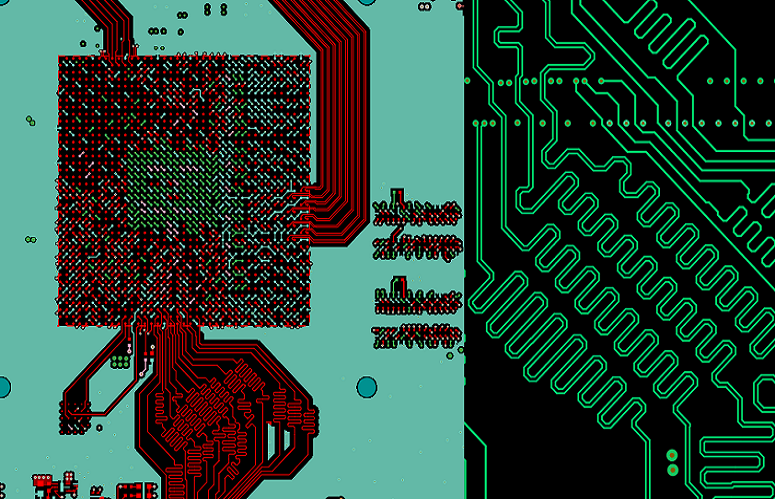
High-speed PCB design for 10G/25G/100G requires
Core Performance Mandates
- 10G Ethernet: 10.3125Gbps, NRZ, Nyquist 5.156GHz, insertion loss ≤15dB.
- 25G Ethernet: 25.78125Gbps, NRZ, Nyquist 12.89GHz, insertion loss ≤22dB.
- 100G Ethernet: 4×25G or 2×50G lanes, PAM4, Nyquist 26GHz, insertion loss ≤28dB.
- Differential impedance: 100Ω ±3% for all Ethernet generations.
- Skew tolerance: ≤5mil (≤2.5ps) for differential pairs, ≤20mil for lane-to-lane.
Structural & Manufacturing Rules
- Minimum layer count: 8 layers for 10/25G; 12-layer symmetric stackup for 100G.
- Trace geometry tolerance: ±0.2mil for width and spacing.
- Warpage limit: ≤0.2mm/m for hdi pcb sequential lamination.
- Copper type: Smooth reverse-treated foil (RTF) to reduce skin-effect loss.
Core Design Principles (10G/25G/100G)
Material Selection
- Standard FR-4: Df ≥0.015, limited to ≤10Gbps, not recommended.
- Low Loss PCB: Df 0.006–0.009, suitable for 10G/25G short channels.
- High frequency pcb: Df 0.002–0.004, mandatory for 100G and long 25G channels.
- Dk stability: ±0.1 across 1–26GHz for consistent impedance.
Learn more about :High-Speed PCB Materials: A Complete Comparison Guide
Impedance Control
- Differential impedance: 100Ω ±3% (IPC-2221 Class 3).
- Single-ended impedance: 50Ω ±3% for clock and control signals.
- Reference plane: Continuous solid ground; no gaps under high-speed traces.
- Impedance coupons: 100mm length on every production panel.
Learn more about: Controlled Impedance in High-Speed PCB: Full Tutorial
Via Management
- Via type: 0.12–0.15mm microvias for hdi pcb; backdrilling required for 25/100G.
- Residual stub: ≤10mil for 25G; ≤5mil for 100G.
- Max vias per lane: 2 transitions for 10/25G; 1 transition for 100G.
- Anti-pad design: 40mil diameter to minimize capacitance.
Routing & Length Matching
Key Routing Guidelines
- Avoid vias: Minimize layer transitions for 100G Ethernet lanes.
- 3W Rule: Trace spacing ≥3× width for 10/25G; 5W Rule for 100G.
- Continuous planes: No routing over splits or slots; eliminate return path gaps.
- Bend rule: 45° or curved bends only; radius ≥3× trace width.
Length Matching
- Intra-pair skew: ≤5mil (≤2.5ps) for all Ethernet speeds.
- Lane-to-lane mismatch: ≤20mil for 10/25G; ≤10mil for 100G.
- Serpentine tuning: Pitch ≥5× trace width to avoid coupling.
- Match segments: Compensate bends and vias individually.
Stack-up Design
Symmetric Layer Configuration
- 8-layer (10/25G): Signal-GND-Power-Signal-Signal-Power-GND-Signal.
- 12-layer (100G): Signal-GND-Signal-GND-Power-GND-Signal-GND-Power-GND-Signal-GND.
- Dielectric thickness: 0.1–0.15mm between signal and ground.
- Plane pair spacing: ≤0.2mm for maximum interplane capacitance.
HDI PCB Stackup Optimization
- 2+N+2 structure with stacked microvias for BGA fanout.
- Alternating signal and ground layers to eliminate broadside crosstalk.
- Symmetric layer arrangement to prevent warpage and impedance shift.
- Copper weight: 1oz (35μm) for signals; 2oz (70μm) for power planes.
Learn more about: High Speed PCB Layer Stackup: Design Guide & Examples
100G Specific Considerations
Modulation & Loss
- 100G Ethernet uses PAM4 modulation, halving voltage margin vs NRZ.
- Insertion loss budget: ≤28dB @26GHz.
- Return loss: ≤-15dB across entire frequency range.
- Equalization: FFE/DFE required for long 100G channels.
Connectors & Transition
- Connector type: SFP28, QSFP28, QSFP-DD with controlled impedance.
- AC coupling capacitors: 0201 size, symmetric placement.
- Trace-to-connector transition: Impedance-matched pad design.
- Guard traces: Grounded vias every 100mil along connector paths.
Validation & Testing
Simulation
- 3D EM simulation for vias, connectors, and bends up to 30GHz.
- S-parameter extraction: Insertion loss, return loss, crosstalk.
- Eye diagram simulation: Include noise, jitter, and crosstalk.
- TDR analysis: Verify impedance continuity and discontinuities.
Testing
- Laboratory measurement: S-parameter test up to 30GHz.
- Eye diagram test: At-speed 100G Ethernet validation.
- Impedance test: TDR with 20ps rise time.
- Thermal cycle test: 1000 cycles (-40°C to 125°C) for reliability.
Key Comparisons
| Parameter | 10G Ethernet | 25G Ethernet | 100G Ethernet |
|---|---|---|---|
| Data Rate | 10.3Gbps | 25.78Gbps | 100Gbps (PAM4) |
| Nyquist Frequency | 5.15GHz | 12.89GHz | 26GHz |
| Max Insertion Loss | ≤15dB | ≤22dB | ≤28dB |
| Recommended Material | Low Loss PCB | Low Loss PCB | High Frequency PCB |
| Max Stub Length | ≤15mil | ≤10mil | ≤5mil |
| Routing Rule | 10/25G | 100G |
|---|---|---|
| Spacing Rule | 3W | 5W |
| Max Vias per Lane | 2 | 1 |
| Skew Tolerance | ≤5mil | ≤3mil |
| Impedance Tolerance | ±5% | ±3% |
Case Study: 12-Layer HDI High Frequency PCB
Project Specifications
- Layers: 12-layer symmetric hdi pcb stackup.
- Protocol: 100G Ethernet (4×25Gbps NRZ).
- Material: High frequency pcb (Df=0.003, Dk=3.4).
- Impedance: 100Ω differential ±3%.
- Trace: 4.0mil width, 5.0mil spacing, stripline.
Issues Encountered
- Insertion loss: 29.4dB @26GHz (exceeded 28dB limit).
- Near-end crosstalk: -26dB (target ≤-35dB).
- Via stub: 18mil causing resonance and return loss loss.
- Impedance variation: ±6% outside specification.
Improvements Implemented
- Upgraded from Low Loss PCB to high frequency pcb.
- Applied backdrilling to reduce stub from 18mil to 4mil.
- Increased spacing from 3W to 5W rule (12mil to 20mil).
- Adjusted trace width to 4.5mil and dielectric to 0.12mm.
- Added ground guard traces with stitching vias every 120mil.
Results
- Insertion loss improved to 26.8dB @26GHz.
- Crosstalk reduced to -36dB.
- Impedance controlled to ±2.7%.
- Return loss improved to -21dB.
- Manufacturing yield increased from 72% to 95.7%.
| Case Study Aspect | Details / Parameters |
|---|---|
| Project Specifications | 12-layer symmetric HDI PCB, 100G Ethernet (4×25Gbps), High Frequency PCB (Df=0.003), 100Ω differential, 4.0mil width, 5.0mil spacing |
| Issues Encountered | Insertion loss 29.4dB@26GHz, crosstalk -26dB, via stub 18mil, impedance ±6% |
| Improvements Implemented | Upgraded to High Frequency PCB, backdrill stub 18→4mil, spacing 3W→5W, trace 4.0→4.5mil, guard traces 120mil via pitch |
| Results | Insertion loss 26.8dB, crosstalk -36dB, impedance ±2.7%, return loss -21dB, yield 72%→95.7% |
Common Design Errors
- Inadequate Material Grade: Using standard FR-4 or Low Loss PCB for 100G causes 30% excess loss and requires full redesign.
- Excessive Via Stub Length: Stubs >10mil create resonance that invalidates 100G compliance and cannot be repaired.
- Violating 3W/5W Spacing: Tight spacing causes crosstalk that cannot be corrected after etching.
- Discontinuous Reference Planes: Routing over gaps increases EMI and insertion loss by 25%.
FAQ
Q1: What material is required for 100G Ethernet high speed pcb?
A1: 100G requires high frequency pcb with Df ≤0.004 and stable Dk up to 26GHz. Low Loss PCB is insufficient for 100G operation.
Q2: What are the via rules for 100G Ethernet in hdi pcb?
A2: Use 0.12–0.15mm microvias with backdrilling to ≤5mil stub. Maximum one via transition per 100G lane.
Q3: What routing rules apply to 100G Ethernet?
A3: Use the 5W spacing rule, minimize vias, maintain continuous ground planes, and match length to ≤3mil skew.
Q4: What insertion loss budget applies to 100G Ethernet?
A4: Total insertion loss must be ≤28dB @26GHz. High frequency pcb materials and short trace lengths are required to meet this budget.
If you need professional high speed PCB impedance design support or quotation, our team provides free DFM check and fast turnaround.


![Understanding PCB Costs & Pricing [Your Complete Guide]](https://hdicircuitboard.com/wp-content/uploads/elementor/thumbs/Understanding-PCB-Costs-Pricing-Your-Complete-Guide-qzzhe6mcaxuolkux3xalfktgavumi9y1aqfbs9bpv4.webp "Understanding PCB Costs & Pricing [Your Complete Guide]")


