
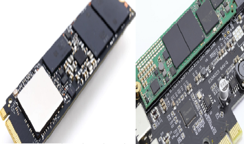
High-speed PCB design for PCIe 5.0 (32 GT/s NRZ) and PCIe 6.0 (64 GT/s PAM4) demands strict loss budgeting, ultra-precise impedance control, low-loss materials, via optimization, and crosstalk mitigation to maintain eye opening and minimize bit error rates. This guide delivers factory-verified parameters, stackup rules, routing constraints, and simulation standards for hdi pcb, Low Loss PCB, and high frequency pcb platforms operating at the PCIe 5.0/6.0 specification limits.
Learn more about: What Is High-Speed PCB? A Comprehensive Guide
Key Design Requirements for PCIe 5.0/6.0
Speed & Signaling Fundamentals
- PCIe 5.0: 32 GT/s, NRZ coding, Nyquist frequency 16 GHz.
- PCIe 6.0: 64 GT/s, PAM4 coding, Nyquist frequency 32 GHz.
- Insertion loss budget: ≤28 dB for PCIe 5.0; ≤20 dB for PCIe 6.0 at Nyquist.
- Minimum eye height: 15 mV after equalization for both generations.
- Minimum eye width: 9.375 ps for PCIe 6.0; 18.75 ps for PCIe 5.0.
Impedance & Tolerance Mandates
- Differential impedance: 85 Ω ±5% for add-in cards; 100 Ω ±5% for mainboards.
- Single-ended impedance: 50 Ω ±5% for clock and control signals.
- Impedance deviation: ≤3% for high frequency pcb operating above 20 GHz.
- Trace geometry tolerance: ±0.2 mil for line width and spacing.
Learn more about: 50Ω / 75Ω / 100Ω Impedance in High Density Interconnect (HDI) PCBs: Design & Production Guide
Low Loss PCB Material Selection
Material Grades & Performance
- Standard FR-4: Df 0.014–0.025, limited to ≤10 GHz, not recommended for PCIe 5.0/6.0.
- Low Loss PCB: Df 0.006–0.009, suitable for PCIe 5.0 short channels.
- Ultra Low Loss PCB: Df 0.002–0.004, required for PCIe 6.0 and long PCIe 5.0 channels.
- High frequency pcb materials: Stable Dk ±0.1 over 1–32 GHz.
Copper & Surface Finish
- Copper type: Reverse-treated foil (RTF) or very smooth copper to reduce skin-effect loss.
- Copper weight: 1 oz (35 μm) for signal layers; 2 oz (70 μm) for power planes.
- Surface finish: Immersion silver or ENEPIG; avoid ENIG due to nickel loss.
- Glass weave: Tight weave construction to minimize skew and impedance variation.
Learn more about : High-Speed PCB Materials: A Complete Comparison Guide
Loss Budget & Insertion Loss Control
Channel Loss Allocation
- Total insertion loss: ≤28 dB @16 GHz for PCIe 5.0.
- Total insertion loss: ≤20 dB @32 GHz for PCIe 6.0.
- Crosstalk allocation: 4–5 dB margin for PCIe 5.0; 6–8 dB for PCIe 6.0.
- Environmental loss margin: 2–3 dB for temperature and humidity variation.
Loss Reduction Methods
- Trace length: ≤8 inches for PCIe 5.0; ≤6 inches for PCIe 6.0 without redrivers.
- Dielectric loss: Minimized by ultra low loss materials.
- Conductor loss: Reduced by smooth copper and optimized trace width.
- Via loss: Limited to ≤0.5 dB per via transition.
Via Optimization & Backdrilling
Via Design Rules
- Via type: Microvias 0.1–0.15 mm for hdi pcb; stacked vias allowed in 2+N+2 stackup.
- Via pad/anti-pad: 10/20/40 rule (drill/pad/anti-pad) for 50/85/100 Ω impedance.
- Via count: Maximum 2 via transitions per PCIe lane.
- Via-in-pad: Required for BGA fanout to minimize stub and parasitics.
Backdrilling Specifications
- Backdrill target: Residual stub ≤5 mil for PCIe 6.0; ≤10 mil for PCIe 5.0.
- Drill bit size: 6–8 mil larger than original via hole.
- Depth tolerance: ±2 mil controlled depth drilling.
- Return loss improvement: 10–15 dB after backdrilling.
Routing Rules for PCIe 5.0/6.0
Differential Pair Routing
- Intra-pair length matching: ≤5 mil (≤2.5 ps skew).
- Inter-pair mismatch: ≤1 inch allowed between lanes.
- Pair spacing: Fixed along entire length; no necking or expansion.
- Bend rule: 45° or curved bends only; radius ≥3× trace width.
Crosstalk Mitigation
- Pair-to-pair spacing: ≥5× width or ≥4× reference plane height.
- Parallel run limit: ≤200 mil continuous parallel between different pairs.
- Guard traces: Grounded vias every 100–150 mil along critical routes.
- Layer routing: Stripline preferred for ≥16 GHz; inner layers only for PCIe 6.0.
Signal Integrity & Simulation
PAM4 Signaling Challenges
- PAM4 has 50% less voltage margin than NRZ, making crosstalk critical.
- Equalization adaptation required for PCIe 6.0 due to higher loss.
- Jitter budget: ≤35 ps for PCIe 5.0; ≤20 ps for PCIe 6.0.
- BER target: 1e-12 for PCIe 5.0; 1e-15 with FEC for PCIe 6.0.
Simulation Requirements
- 3D electromagnetic simulation for vias, connectors, and bends.
- Post-layout S-parameter extraction up to 40 GHz.
- Eye diagram simulation with channel loss and crosstalk included.
- TDR analysis for impedance discontinuity verification.
Practical Layout Considerations
Connector & AC Coupling
- Connector type: PCIe CEM edge fingers with controlled impedance design.
- AC coupling capacitor: 0201 size, 100–220 nF, placed near receiver.
- Reference plane void: 100% clearance under capacitor pads.
- Via placement: Symmetric for both sides of differential pair.
Stackup & Shielding
- Layer count: Minimum 8 layers for PCIe 5.0; 12 layers recommended for PCIe 6.0.
- Stackup structure: Signal-GND-Power-Signal-Signal-Power-GND-Signal.
- Symmetric layer arrangement to prevent warpage ≤0.2 mm/m.
- Ground stitching vias: 1 mm pitch along differential pair routes.
Key Comparisons
| Parameter | PCIe 5.0 (32 GT/s) | PCIe 6.0 (64 GT/s) |
|---|---|---|
| Signaling | NRZ | PAM4 |
| Nyquist Frequency | 16 GHz | 32 GHz |
| Insertion Loss Budget | ≤28 dB @16 GHz | ≤20 dB @32 GHz |
| Minimum Eye Width | 18.75 ps | 9.375 ps |
| Max Stub Length | ≤10 mil | ≤5 mil |
| Recommended Material | Low Loss PCB | Ultra Low Loss PCB |
| Material Type | Df @10GHz | Max Frequency | PCIe Generation |
|---|---|---|---|
| Standard FR-4 | 0.018 | ≤10 GHz | Not Supported |
| Low Loss PCB | 0.006–0.009 | 16 GHz | PCIe 5.0 |
| Ultra Low Loss PCB | 0.002–0.004 | 32+ GHz | PCIe 5.0/6.0 |
Case Study: 12-Layer HDI Ultra Low Loss PCB
Project Specifications
- Layers: 12-layer symmetric hdi pcb stackup.
- Speed: PCIe 6.0 (64 GT/s PAM4).
- Material: Ultra low loss pcb (Df=0.0025, Dk=3.4).
- Impedance: 85 Ω differential, ±3% tolerance.
- Trace: 4.2 mil width, 5 mil spacing, stripline inner layers.
Issues Encountered
- Insertion loss reached 22.4 dB @32 GHz (exceeded 20 dB limit).
- Near-end crosstalk reached -28 dB (target ≤-35 dB).
- Via stub caused return loss degradation to -10 dB.
- Impedance variation reached ±7% outside specification.
Improvements Implemented
- Changed from low loss to ultra low loss material.
- Applied backdrilling to reduce stub from 18 mil to 4 mil.
- Increased pair-to-pair spacing from 3× to 5× width.
- Adjusted trace width to 4.5 mil and optimized stackup thickness.
- Added ground guard traces with stitching vias every 120 mil.
Results
- Insertion loss improved to 18.6 dB @32 GHz (compliant).
- Crosstalk reduced to -36 dB.
- Return loss improved to -22 dB.
- Impedance controlled to ±2.8%.
- Manufacturing yield improved from 76% to 95.8%.
| Case Study Aspect | Details / Parameters |
|---|---|
| Project Specifications | 12-layer symmetric HDI PCB, PCIe 6.0 (64 GT/s PAM4), Ultra Low Loss PCB (Df=0.0025), 85Ω differential, 4.2mil width, 5mil spacing |
| Issues Encountered | Insertion loss 22.4dB@32GHz (over 20dB limit), crosstalk -28dB (target ≤-35dB), via stub return loss -10dB, impedance ±7% |
| Improvements Implemented | Upgraded to Ultra Low Loss PCB, backdrill stub 18→4mil, spacing 3×→5× width, trace 4.2→4.5mil, added guard traces with 120mil stitching vias |
| Results | Insertion loss 18.6dB@32GHz, crosstalk -36dB, return loss -22dB, impedance ±2.8%, yield 76%→95.8% |
Common Design Errors
- Inadequate Material Grade: Using standard FR-4 or low-loss material for PCIe 6.0 leads to 30% excess loss and requires full redesign.
- Insufficient Via Stub Control: Stubs longer than 10 mil create resonance and return loss failure, requiring costly rework.
- Pair Spacing Too Tight: Less than 4× reference plane height causes severe crosstalk that cannot be corrected after fabrication.
- Asymmetric Stackup: Causes warpage ≥0.7 mm/m, leading to impedance shift and low production yield.
Quality Control & Compliance
Testing Protocols
- Impedance test: TDR measurement with 20 ps rise time.
- S-parameter test: Up to 40 GHz for insertion and return loss.
- Crosstalk measurement: NEXT and FEXT characterization.
- Eye diagram verification: At-speed testing with real PCIe 6.0 hardware.
Standards Compliance
- PCI-SIG PCIe 5.0/6.0 specification.
- IPC-2221: Generic PCB design standard.
- IPC-6012 Class 3: High-performance rigid PCB requirements.
- CISPR 22 Class B: Radiated emission limits.
FAQ
Q1: What material is required for PCIe 6.0 high speed pcb?
A1: PCIe 6.0 requires ultra low loss pcb with Df ≤0.004 and stable Dk up to 32 GHz. Low Loss PCB is insufficient and causes excessive insertion loss at 64 GT/s.
Q2: What are the via rules for PCIe 5.0/6.0 in hdi pcb?
A2: Use via-in-pad with 0.12–0.15 mm microvias. Backdrill to residual stub ≤5 mil for PCIe 6.0 and ≤10 mil for PCIe 5.0. Max 2 vias per lane.
Q3: How much crosstalk is allowed for PCIe 6.0?
A3: Total crosstalk must be ≤-35 dB. Pair-to-pair spacing must be ≥5× trace width or ≥4× reference plane height to meet this requirement.
Q4: What impedance is required for PCIe 5.0/6.0 add-in-cards?
A4: Add-in-cards require 85 Ω differential impedance ±5%. Mainboard designs use 100 Ω differential impedance. Both require tight tolerance for PCIe 6.0 operation.
If you need professional high speed PCB impedance design support or quotation, our team provides free DFM check and fast turnaround.


![Understanding PCB Costs & Pricing [Your Complete Guide]](https://hdicircuitboard.com/wp-content/uploads/elementor/thumbs/Understanding-PCB-Costs-Pricing-Your-Complete-Guide-qzzhe6mcaxuolkux3xalfktgavumi9y1aqfbs9bpv4.webp "Understanding PCB Costs & Pricing [Your Complete Guide]")


