
How to Choose Between Microvias, Stacked Vias, and Staggered Vias for HDI PCBs?
High density interconnect (HDI) PCBs rely on specialized via structures to achieve compactness, high performance, and reliable layer-to-layer connectivity. Microvias, stacked vias, and staggered vias are the three foundational interconnect solutions in HDI design, each optimized for distinct tradeoffs between density, signal integrity, cost, and manufacturability. The choice between them hinges on design requirements like layer count, component pitch, signal speed, application environment, and production volume. This guide breaks down each via type, key decision factors, and practical selection frameworks, adhering to IPC standards (IPC-T-50M, IPC-2226, IPC-6012) to ensure alignment with global manufacturing benchmarks and real-world applicability for electronic engineers.
Learn more about: How to Design HDI Microvia PCB
Microvias – The Foundation of HDI Connectivity
Microvias are the building blocks of HDI technology, defined by IPC-T-50M as blind vias with a maximum aspect ratio of 1:1, depth not exceeding 0.25mm, and diameter typically ranging from 50μm to 150μm. Fabricated via laser drilling (UV or CO2 lasers), they connect adjacent layers and enable the fine-pitch routing critical for modern miniaturized devices.
Core Characteristics & Technical Specifications
- Physical attributes: Diameter 50–150μm (ideal 80–100μm for mass production), aspect ratio ≤0.8:1 for reliable plating, and single-layer connectivity (outer to inner or inner to inner).
- Fabrication process: Laser ablation creates clean, precise holes without mechanical stress; plating via electroless copper deposition followed by electrolytic copper ensures conductivity, with optional resin or copper filling for via-in-pad (VIP) applications.
- Key standards compliance: IPC-2226 specifies minimum annular ring dimensions (250μm for Class 2, 325μm for Class 3) and dielectric thickness (60–80μm between connected layers).
Ideal Use Cases & Practical Advantages
- Target applications: Entry-level HDI (1+N+1 stackups), low-to-mid density designs, cost-sensitive consumer electronics (mid-range smartphones, wearables), IoT sensors, and basic industrial controllers.
- User-centric benefits:
- Enables 0.4mm pitch BGA fanout without layer count bloat, replacing 6-layer conventional PCBs with 4-layer HDI.
- Reduces parasitic capacitance and inductance by 50–70% compared to through-hole vias, improving signal integrity for frequencies up to 5GHz.
- Simplifies manufacturing with high yields (85–95%) and compatibility with standard HDI fabrication workflows.
Limitations & Quality Control
- Constraints: Limited to single-layer connections; unsuitable for ultra-fine pitch components (<0.3mm) or high-speed signals (>10Gbps) requiring multi-layer vertical paths.
- Quality control measures: Mandatory automated optical inspection (AOI) and X-ray inspection to detect plating voids; cross-sectional analysis to verify copper thickness (minimum 12μm) and absence of glass fiber protrusion in via walls.
Stacked Vias – Maximum Density for High-Performance Designs
Stacked vias are vertically aligned microvias stacked across multiple build-up layers, creating a direct vertical interconnect path through 3+ layers. They are the gold standard for ultra-compact, high-density HDI designs, where space efficiency and signal path minimization are non-negotiable.
Core Characteristics & Technical Specifications
- Physical attributes: Stacked microvias (50–100μm diameter) aligned with ±20μm positional tolerance; requires copper filling and planarization to support subsequent layers.
- Fabrication process: Built via Sequential Lamination (2+ cycles), with each layer’s microvias drilled, plated, filled, and planarized before adding the next layer; relies on laser direct imaging (LDI) for precise alignment.
- Key standards compliance: IPC-6016 mandates 100% copper filling for stacked vias; IPC-2226 limits stack height to 2–3 microvias to avoid reliability risks.
Ideal Use Cases & Practical Advantages
- Target applications: High-end HDI (2+N+2 or any-layer stackups), flagship consumer electronics (premium smartphones, GPUs), 5G base stations, AI accelerators, and medical implants.
- User-centric benefits:
- Supports 0.2–0.3mm pitch BGAs with >300 pins, reducing board area by 30–40% compared to staggered vias.
- Minimizes signal path length, enabling signal integrity for data rates >10Gbps (e.g., DDR5, PCIe 5.0) by eliminating stub effects and impedance discontinuities.
- Enables multi-layer connectivity without horizontal routing, freeing up surface space for additional components.
Limitations & Quality Control
- Constraints: Higher cost (25–40% premium over microvias) due to complex fabrication; lower yields (70–85%) from strict alignment and filling requirements.
- Quality control measures: TDR (Time-Domain Reflectometry) testing for impedance consistency; thermal cycling tests (–40°C to +125°C, 1,000 cycles) to detect joint separation; microsection analysis to ensure zero voids in copper filling.
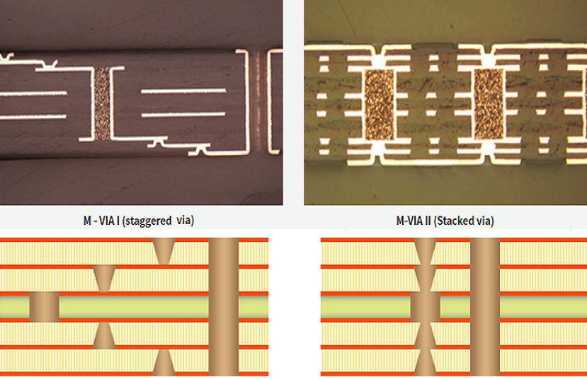
Staggered Vias – Balancing Reliability, Cost, and Density
Staggered vias are offset microvias across layers, connected by short internal traces instead of direct vertical alignment. They strike a middle ground between microvias and stacked vias, prioritizing reliability and manufacturability while delivering moderate density gains.
Core Characteristics & Technical Specifications
- Physical attributes: Microvias (75–125μm diameter) offset by ≥via diameter; vertical spacing between centers exceeds 400μm (recommended) to avoid mechanical stress.
- Fabrication process: Uses single or dual Sequential Lamination cycles; no mandatory copper filling (only outer-layer vias require filling), reducing process complexity compared to stacked vias.
- Key standards compliance: IPC-2226 specifies minimum trace width (4mil) between offset vias; IPC-6012 Class 2 allows staggered vias for industrial and automotive applications.
Ideal Use Cases & Practical Advantages
- Target applications: Mid-tier HDI (2+N+2 stackups), automotive ADAS, industrial controllers, ruggedized electronics, and high-volume production where reliability is critical.
- User-centric benefits:
- Delivers 20–30% higher density than microvias while maintaining yields of 80–90%, reducing scrap costs in volume production.
- Distributes thermal and mechanical stress across layers, surviving 2x more thermal cycles (2,000+ vs. 1,000) than stacked vias in harsh environments.
- Balances cost and performance, with a 15–20% cost premium over microvias (vs. 25–40% for stacked vias).
Limitations & Quality Control
- Constraints: Requires 10–15% more board space than stacked vias; introduces minor impedance discontinuities, making it unsuitable for signals >25Gbps.
- Quality control measures: Impedance testing to verify continuity across offset traces; vibration testing (10–2,000Hz, 10g rms) for automotive/industrial applications; AOI to detect trace-width variations.
Key Decision Factors – Comparing the Three Via Types
The selection of microvias, stacked vias, or staggered vias depends on five non-negotiable design and production criteria, each directly impacting performance, cost, and scalability.
Density & Space
| Via Type | Maximum Component Pitch | Board Area Efficiency | Layer Count Reduction |
|---|---|---|---|
| Microvias | 0.4mm | Moderate (120–160 pins/sq.in) | 20–30% |
| Stacked Vias | 0.2–0.3mm | High (200–300 pins/sq.in) | 40–50% |
| Staggered Vias | 0.3–0.4mm | Moderate-High (160–200 pins/sq.in) | 30–40% |
Signal Integrity
- Microvias: Suitable for signals <5GHz; minimal parasitic effects (0.1–0.2pF capacitance) ideal for low-to-mid speed digital and analog circuits.
- Stacked Vias: Optimal for signals >10Gbps; shortest signal path minimizes reflection and attenuation, critical for 5G mmWave and high-speed memory interfaces.
- Staggered Vias: Balanced for 5–25GHz signals; minor impedance discontinuities (±5%) manageable with proper trace design.
Cost & Yield
| Via Type | Cost vs. Conventional PCBs | Production Yield | Volume Cost Scalability |
|---|---|---|---|
| Microvias | +10–15% | 85–95% | Excellent (25% cost reduction at 10k+ units) |
| Stacked Vias | +60–80% | 70–85% | Limited (10–15% cost reduction at 10k+ units) |
| Staggered Vias | +30–40% | 80–90% | Good (20% cost reduction at 10k+ units) |
Manufacturing & Reliability
- Manufacturing complexity: Microvias (low) → Staggered vias (moderate) → Stacked vias (high); stacked vias require specialized equipment (horizontal plating lines, LDI) and skilled operators.
- Reliability in harsh environments: Staggered vias (highest) → Microvias → Stacked vias (lowest); stacked vias are prone to corner cracking in thermal cycling due to CTE mismatch.
Practical Selection Framework – Step-by-Step Guidance
Start with Microvias for 1+N+1 HDI, Low-Cost, Low-to-Mid Density
Choose microvias if:
- PCB stackup is 1+N+1 (entry-level HDI) with 4–8 layers.
- Component pitch is ≥0.4mm, and signal frequency <5GHz.
- Project prioritizes cost efficiency and high production yields (e.g., consumer electronics, IoT sensors).
- Example: A 4-layer (1+2+1) HDI for a mid-range tablet, supporting a 0.4mm pitch BGA with 150 pins.
Upgrade to Stacked Vias for 2+N+2/Any-Layer, <0.3mm Pitch, >10Gbps, Extreme Miniaturization
Choose stacked vias if:
- PCB stackup is 2+N+2 or any-layer (high-end HDI) with 8–20 layers.
- Component pitch is ≤0.3mm (e.g., ultra-fine BGAs, chiplets), and signal speed >10Gbps.
- Device size is a hard constraint (e.g., smartphones, implantable medical devices).
- Example: A 12-layer any-layer HDI for a flagship smartphone, accommodating a 0.2mm pitch BGA with 800+ pins and 5G mmWave signals.
Choose Staggered Vias for 2+N+2 HDI, Industrial/Automotive, Cost-Reliability Balance, and Higher Yield
Choose staggered vias if:
- PCB stackup is 2+N+2 (mid-tier HDI) with 6–12 layers.
- Application operates in harsh environments (automotive, industrial, aerospace) requiring vibration and thermal resistance.
- Project needs a balance of density, cost, and yield (e.g., ADAS modules, industrial controllers).
- Example: An 8-layer (2+4+2) HDI for an automotive infotainment system, supporting 0.35mm pitch BGAs and surviving under-hood temperature fluctuations.
Long-Tail Considerations & FAQ
PCB vs. PCA – How Via Selection Impacts Assembly
- Microvias: Compatible with standard SMT assembly; no additional process costs.
- Stacked Vias: May require thermocompression bonding for flip-chip components; assembly cost +20–30%.
- Staggered Vias: Supports both SMT and through-hole assembly; minor cost premium (+10–15%) for fine-pitch placement.
How to Optimize Via Design for Manufacturability
- Use hybrid via strategies: Microvias in low-density areas, stacked/staggered vias in high-density BGA regions.
- Specify the largest feasible via diameter (e.g., 100μm vs. 75μm) to improve plating reliability and yield.
- Collaborate with HDI manufacturers early to align via design with Design for Manufacturability (DFM) guidelines, avoiding overly tight tolerances.
When to Combine Via Types in a Single Design
Hybrid via designs are common in complex HDI boards:
- Use stacked vias for BGA fanout (dense center area).
- Use staggered vias for peripheral routing (balance of density and reliability).
- Use microvias for non-critical signals (cost efficiency).
- Example: A 10-layer HDI for a data center switch, combining stacked vias for GPU fanout, staggered vias for networking ports, and microvias for power delivery.
Conclusion
The choice between microvias, stacked vias, and staggered vias is a critical decision that defines an HDI PCB’s density, performance, cost, and reliability. Microvias serve as the cost-effective foundation for entry-level HDI, while stacked vias deliver the extreme density and signal integrity required for next-gen electronics. Staggered vias fill the gap for applications needing a balance of performance, cost, and ruggedness—particularly in industrial and automotive sectors. By aligning via selection with stackup type (1+N+1, 2+N+2, any-layer), component pitch, signal speed, and application environment, design and procurement teams can optimize HDI designs for manufacturability and end-use performance. Adherence to IPC standards, early collaboration with HDI manufacturers, and a clear understanding of tradeoffs ensure that via selection drives value rather than compromise. Whether designing a cost-sensitive IoT sensor or a high-performance 5G device, the right via strategy turns HDI’s complexity into a competitive advantage.


