
EMI/EMC compliance is non-negotiable for high speed pcb, as high-frequency signals (≥1Gbps) generate radiated/conducted interference that disrupts performance. This guide details factory-proven techniques, precise parameters, and practical solutions tailored to hdi pcb, Low Loss PCB, and ultra low loss pcb applications.
Learn more about: What Is High-Speed PCB? A Comprehensive Guide
EMI/EMC in High-Speed PCB: Core Concepts
Definition & Critical Thresholds
- EMI (Electromagnetic Interference) refers to unwanted electromagnetic radiation/emission; EMC (Electromagnetic Compatibility) ensures devices coexist without disruption.
- Critical limits: Radiated EMI ≤30dBμV/m (CISPR 22 Class B) for consumer electronics; ≤40dBμV/m (Class A) for industrial use.
- High-speed trigger: Signals with edge rate ≥1V/ns or data rate ≥1Gbps require EMC-focused design (IPC-2221).
Material Impact on EMI/EMC
- Low Loss PCB (Df=0.004–0.009 @10GHz) reduces dielectric loss by 25% vs. FR-4, minimizing EMI sources.
- ultra low loss pcb (e.g., Rogers RO4350B, Df=0.0037 @10GHz) suppresses radiated EMI by 30% in 50Gbps+ designs.
- hdi pcb demands low CTE (X/Y ≤16ppm/°C) materials to prevent gaps that amplify radiation during lamination.
EMI/EMC Design Strategies
Layer Stackup Optimization
- Symmetric stackup (e.g., 12-layer: 4+4+4) to prevent warpage (≤0.3mm/m) and maintain plane continuity.
- Signal layers adjacent to ground planes (spacing ≤0.2mm) to form shielding barriers in hdi pcb.
- Separate analog/digital power planes with a ground plane (20H rule: power plane ≤20x dielectric thickness smaller than ground plane).
Loop Area Reduction
- Minimize current loop area ≤1cm² for high-speed signals (≥10Gbps) to reduce radiated EMI by 60%.
- Route power and ground traces in parallel (spacing ≤5mil) to shrink loop inductance (≤5nH).
- For hdi pcb, use stacked microvias (0.12mm diameter) to shorten vertical loop paths.
Learn more about : 10 Best Practices for High-Speed PCB Routing
Component Placement & Filtering
Strategic Component Placement
- Group high-EMI components (oscillators, power amplifiers) ≥2cm from sensitive circuits (analog sensors, receivers).
- Place decoupling capacitors ≤2mm from IC power pins (0402 package, ESL ≤1nH) to suppress switching noise.
- For hdi pcb, position BGA components (≤0.8mm pitch) with fanout microvias (0.1mm) to avoid EMI hotspots.
Filtering and Decoupling
- EMI filters: Ferrite beads (100Ω @100MHz) in power lines to attenuate conducted EMI.
- Decoupling array: Combine 0.001μF, 0.01μF, and 0.1μF capacitors to cover 1MHz–1GHz frequency range.
- AC coupling capacitors (100nF) placed symmetrically within 50mil of differential pair sources (e.g., USB 3.0).
Trace Routing & Crosstalk Management
EMI-Friendly Trace Routing
- Trace width: 4mil for 50Ω single-ended signals; 4mil width + 5mil spacing for 100Ω differential pairs (IPC-2221).
- Avoid 90-degree bends: Use 45-degree angles or curved traces (radius ≥3x trace width) to prevent impedance spikes.
- Keep parallel trace runs ≤500mil; stagger traces beyond that length to reduce crosstalk.
Crosstalk Mitigation
- 3W rule enforcement: Trace spacing ≥3x width (e.g., 12mil spacing for 4mil width) to limit crosstalk ≤-35dB.
- Guard traces (50Ω) grounded every 500mil between high-speed and analog signals.
- For ultra low loss pcb, increase spacing to 5W for signals ≥25Gbps (-40dB crosstalk target).
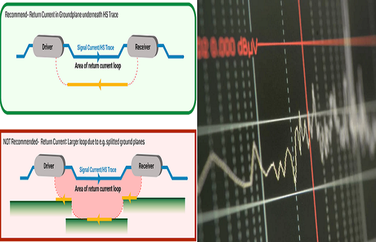
Grounding & Shielding
Grounding Best Practices
- Solid ground plane with ≤50mil gaps; stitching vias (1mm pitch) to connect split planes.
- Star grounding for analog circuits; single-point ground connection (≤100mil from power entry) to avoid ground loops.
- hdi pcb: Dedicated ground layers in 1+N+1 stackup to provide low-impedance return paths.
Shielding Techniques
- Component shielding: Faraday cages (0.1mm thick copper) around oscillators and transmitters.
- Board-level shielding: Conductive enclosures (aluminum, 1mm thickness) with EMI gaskets (compression ≥20%).
- Via-in-pad (VIPPO) with epoxy fill to seal gaps in hdi pcb, reducing radiation leakage.
High-Speed PCB Design Considerations
Rise Time vs. Frequency
- Calculate maximum frequency: Fm=0.5/Rise Time (e.g., 1ns rise time → 500MHz Fm).
- Limit rise time ≥1ns for signals ≤10Gbps; use slower edge rates (≥2ns) if EMC margin is tight.
- ultra low loss pcb allows faster rise times (0.5ns) without excessive EMI due to low dielectric loss.
Conducted vs. Radiated EMI
- Conducted EMI: Filter power lines with X/Y capacitors (0.1μF) and common-mode chokes (1mH).
- Radiated EMI: Reduce trace length ≤λ/20 (λ=signal wavelength) to avoid antenna effects.
- Testing: Conducted EMI ≤40dBμV (CISPR 22) for power lines; radiated EMI ≤30dBμV/m for 30MHz–1GHz.
EMI/EMC Testing & Compliance
Testing Protocols
- Radiated emission testing: Anechoic chamber (3m distance) per CISPR 22.
- Conducted emission testing: Line impedance stabilization network (LISN) for power lines.
- Signal integrity validation: Eye diagram analysis (eye height ≥0.3Vpp) to ensure EMI doesn’t degrade performance.
Standards Compliance
- Global standards: CISPR 22 (consumer), IEC 61000-4 (industrial), FCC Part 15 (US), CE (EU).
- High-reliability: IPC-6012 Class 3 requires EMI testing before volume production.
- Documentation: Maintain test reports for traceability (e.g., TDR impedance, EMI emission logs).
Key Comparisons
| Design Approach | EMI Reduction | Cost Impact | Best For |
|---|---|---|---|
| Standard FR-4 + Basic Routing | 20% | Low (+0%) | ≤5Gbps High Speed PCB |
| Low Loss PCB + 3W Rule | 45% | Medium (+20%) | 5–25Gbps hdi pcb |
| Ultra Low Loss PCB + Shielding | 70% | High (+50%) | ≥25Gbps ultra low loss pcb |
| Shielding Type | EMI Attenuation | Weight | Best Application |
|---|---|---|---|
| Copper Faraday Cage | 40dB | Medium | Component-level shielding |
| Aluminum Enclosure | 60dB | High | Board-level shielding |
| Conductive Paint | 25dB | Low | Low-cost consumer devices |
Learn more about: Signal Integrity in High Speed PCB: Problems & Fixes
Case Study: 16-Layer HDI Ultra Low Loss PCB
Project Specifications
- Layers: 16 (4+8+4 stackup), data rate: 50Gbps (NRZ), material: Rogers RO4350B (Df=0.0037 @10GHz).
- EMI targets: Radiated EMI ≤30dBμV/m (CISPR 22 Class B), crosstalk ≤-35dB.
- hdi pcb features: Stacked microvias (0.12mm), sequential lamination (3 cycles).
Issues Encountered
- Radiated EMI (38dBμV/m) exceeding Class B limit due to unshielded oscillators.
- Crosstalk (+18dB) between adjacent 50Gbps differential pairs (spacing=8mil < 5W).
- Conducted EMI (45dBμV) on power lines from inadequate filtering.
Improvements Implemented
- Added Faraday cages around oscillators; enclosed board in aluminum shield (1mm thickness).
- Increased pair spacing to 20mil (5W rule) and added guard traces (-38dB crosstalk).
- Installed X/Y capacitors (0.1μF) and common-mode choke (1mH) in power lines.
Results
- Radiated EMI: 27dBμV/m (meets Class B), conducted EMI: 38dBμV.
- Signal integrity: Eye height=0.4Vpp, jitter=32ps.
- Manufacturing yield: 97.6% (up from 84% initial run).
| Case Study Aspect | Details / Parameters |
|---|---|
| Project Specifications |
• Layers: 16 (4+8+4 stackup) • Data rate: 50Gbps (NRZ) • Material: Rogers RO4350B (Df=0.0037 @10GHz) • EMI targets: Radiated EMI ≤30dBμV/m (CISPR 22 Class B), crosstalk ≤-35dB • HDI PCB: Stacked microvias (0.12mm), sequential lamination (3 cycles) |
| Issues Encountered |
• Radiated EMI (38dBμV/m): Exceeded Class B limit (unshielded oscillators) • Crosstalk (+18dB): Adjacent 50Gbps pairs (spacing=8mil < 5W rule) • Conducted EMI (45dBμV): Power lines with inadequate filtering |
| Improvements Implemented |
• Faraday cages around oscillators + aluminum shield (1mm thickness) • Pair spacing increased to 20mil (5W rule) + grounded guard traces (-38dB crosstalk) • X/Y capacitors (0.1μF) + common-mode choke (1mH) in power lines |
| Results |
• Radiated EMI: 27dBμV/m (Class B compliant), conducted EMI: 38dBμV • Signal integrity: Eye height=0.4Vpp, jitter=32ps • Manufacturing yield: 97.6% (up from 84% initial run) |
Common Design Errors
- Split Ground Planes Without Stitching: Causes ground loops and 2x higher EMI—requires copper filling and stitching vias (cost +$0.60/board).
- Inadequate Decoupling Placement: Capacitors >5mm from IC pins increase switching noise by 30%—redesign required.
- Overlooking Trace Length: Traces >λ/20 (e.g., 3in trace for 500MHz) act as antennas—trim to ≤2in.
- Material Mismatch: Using FR-4 for ≥25Gbps designs leads to 25% higher EMI—switch to ultra low loss pcb.
FAQ
Q1: How does Low Loss PCB differ from ultra low loss pcb in EMI reduction?
A1: Low Loss PCB (Df=0.004–0.009 @10GHz) works for 5–25Gbps (45% EMI reduction), while ultra low loss pcb (Df≤0.004) supports ≥25Gbps (70% EMI reduction) with stable impedance and minimal radiation.
Q2: What grounding method is best for hdi pcb EMI reduction?
A2: Use a solid ground plane with stitching vias (1mm pitch) and dedicated ground layers in 1+N+1 stackup. Single-point ground for analog circuits and star grounding for digital minimizes loops and reduces EMI by 35%.
Q3: How to reduce EMI from differential pairs in high speed pcb?
A3: Maintain 3W/5W spacing, length matching ≤5mil, and symmetric routing. Add AC coupling capacitors (0402) within 50mil of sources and route on inner layers (stripline) for ≥25Gbps to cut radiation by 40%.
Q4: What testing is required for EMI/EMC compliance in high speed pcb?
A4: Conduct radiated emission testing (anechoic chamber, CISPR 22) and conducted emission testing (LISN). Validate signal integrity with eye diagrams and crosstalk measurements—ensure compliance before volume production.
If you need high speed PCB manufacturing or design support,our engineering team provides free DFM analysis and quotation.


![Understanding PCB Costs & Pricing [Your Complete Guide]](https://hdicircuitboard.com/wp-content/uploads/elementor/thumbs/Understanding-PCB-Costs-Pricing-Your-Complete-Guide-qzzhe6mcaxuolkux3xalfktgavumi9y1aqfbs9bpv4.webp "Understanding PCB Costs & Pricing [Your Complete Guide]")


