How To Route HDI PCB: Expert Strategies for Reliable High Density Interconnect Design
HDI PCB routing demands precision to balance density, signal integrity, and manufacturability—especially for rigid flex pcb, HDI flexible pcb, HDI rigid flex pcb, rf pcb, and multilayer pcb. This guide, built on two decades of HDI design experience and alignment with IPC standards (IPC-2226, IPC-6012), breaks down routing strategies, addresses core challenges, and delivers actionable solutions to ensure HDI circuit boards meet performance and cost goals without compromising on reliability.
Key HDI Routing Strategies and Guidelines
Effective HDI routing starts with foundational strategies that align with microvia technology, stackup design, and component density requirements—critical for avoiding rework and performance failures in high density interconnect applications.
Learn more about: How to Design HDI Microvia PCB
Prioritize Routing Order by Signal Criticality
Routing sequence directly impacts signal integrity and routing efficiency, especially in dense multilayer pcb:
- Critical RF signals (rf pcb): Route first to maintain controlled impedance (±5% tolerance per IPC-2226) and minimize crosstalk. Use shielded traces or differential pairs with consistent spacing.
- High-speed digital signals (≥10Gbps): Follow RF signals to preserve timing budgets. Avoid vias in signal paths; if necessary, use back-drilled blind vias to reduce stub length <300μm.
- Power distribution network (PDN) traces: Route next to ensure low impedance paths (≤0.1Ω) and minimize voltage drop. Use wide traces or copper planes for high-current paths.
- Low-speed control signals: Route last, leveraging remaining space without compromising critical paths.
Optimize Trace Width and Spacing
Trace dimensions balance current capacity, signal integrity, and density—core to HDI pcb routing success:
- Standard HDI (3–4mil trace/space): 0.075mm (3mil) trace / 0.075mm (3mil) space for general signals; supports 0.5A current (1oz copper).
- Ultra HDI (2mil trace/space): 0.05mm (2mil) trace / 0.05mm (2mil) space for dense areas; limited to 0.25A current (1oz copper).
- Power traces: Calculate width based on current (e.g., 0.2mm (8mil) for 1A, 0.4mm (16mil) for 2A) to prevent overheating.
- RF pcb traces: Use impedance-controlled widths (e.g., 0.15mm (6mil) for 50Ω impedance on 0.08mm dielectric) to minimize signal loss.
Tolerance control: Maintain trace width tolerance ±10% for standard HDI, ±5% for ultra HDI (per IPC-6012 Class 3) to ensure consistent performance.
Leverage Microvia and Blind Via Technology
Microvias (≤0.15mm diameter) and blind vias enable high density interconnect by reducing vertical space usage:
- Stacked microvias: Connect 2–4 layers vertically, ideal for multilayer pcb with 8+ layers. Maintain 0.1mm (4mil) clearance between stacked vias.
- Staggered microvias: Avoid vertical alignment to reduce dielectric stress; use for high-speed signals to minimize crosstalk.
- Blind vias: Terminate at internal layers to eliminate stubs; critical for rf pcb and high-speed digital signals (≥25Gbps).
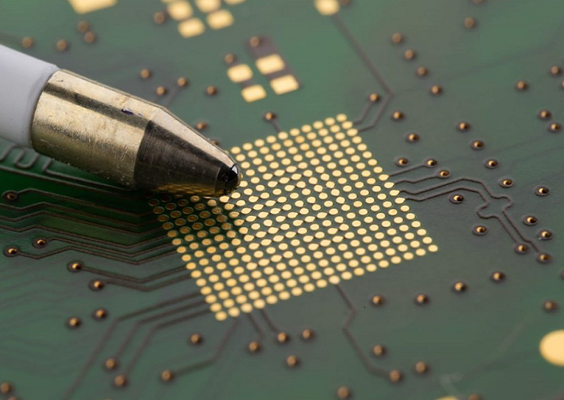
- Via-in-Pad (VIP) technology: Integrate vias directly under BGA pads to save space; fill with solder mask or copper for thermal conductivity.
BGA Fanout & Escape Routing
BGA fanout and escape routing resolve density challenges in fine-pitch components (≤0.4mm pitch):
- Fanout strategy: Use 1:1 fanout (one microvia per BGA pad) for pitches ≤0.5mm. For ≤0.4mm pitch, use staggered microvias to escape traces.
- Escape angle: Route traces at 45° or 90° to avoid acute angles, which cause signal reflections. Maintain 0.05mm (2mil) clearance from BGA pads.
- Layer transition: Escape BGA signals to inner layers within 2–3mm of the component to free up top/bottom layers for other components.
- HDI rigid flex pcb adaptation: For flexible sections, use curved traces (minimum radius = 3x trace width) to prevent trace cracking during bending.
Power Distribution Network (PDN) Optimization
PDN optimization ensures stable power delivery in high-density HDI pcb:
- Decoupling capacitor placement: Position 0.1μF and 10μF capacitors within 0.5mm of BGA power pins to reduce decoupling impedance.
- Power plane design: Use split power planes for multiple voltage domains (e.g., 3.3V, 1.8V) with 0.1mm (4mil) clearance between planes.
- Via placement: Add multiple vias (minimum 2) for power plane transitions to reduce current density <5A/mm².
- Thermal relief: Implement 4-point thermal relief for power pads to balance heat dissipation and solderability.
Sequential Lamination & Stackups for HDI Routing
Sequential lamination enables complex layer structures that support HDI routing, with stackup design directly impacting routing flexibility and signal integrity.
Stackup Design Principles
- Symmetrical stackup: Use balanced layer configurations (e.g., signal-dielectric-ground-ground-dielectric-signal) to minimize warpage during lamination—critical for HDI flexible pcb and HDI rigid flex pcb.
- Dielectric thickness: Maintain 0.05–0.1mm dielectric between signal and ground layers for impedance control. For rf pcb, use thinner dielectrics (0.03–0.05mm) to reduce signal loss.
- Layer count optimization: UHDI designs use 30% fewer layers than standard HDI; a 12-layer UHDI board can replace an 18-layer standard HDI board for the same density.
- Flexible section integration: For HDI rigid flex pcb, use 2–4 signal layers with polyimide dielectric (0.025–0.05mm thick) in flexible sections to preserve bendability.
Sequential Lamination Impact on Routing
- Layer-by-layer routing: Sequential lamination allows routing between newly added layers, enabling any-layer interconnects for high density interconnect.
- Microvia alignment: Each lamination step requires ±0.005mm alignment accuracy to ensure stacked microvia registration—critical for avoiding interlayer shorts.
- Resin flow control: Controlled resin flow (20–30%) fills gaps between layers without covering microvias or traces, preserving routing paths.
Example 8-layer HDI stackup for rf pcb:
- Top signal layer (1oz copper) + 0.05mm low-loss dielectric
- Ground layer (1oz copper) + 0.05mm low-loss dielectric
- Signal layer (1oz copper) + 0.03mm low-loss dielectric
- Power layer (2oz copper) + 0.03mm low-loss dielectric
- Power layer (2oz copper) + 0.03mm low-loss dielectric
- Signal layer (1oz copper) + 0.05mm low-loss dielectric
- Ground layer (1oz copper) + 0.05mm low-loss dielectric
- Bottom signal layer (1oz copper)
Microvia Reliability in HDI Routing
Microvia reliability is critical for long-term HDI pcb performance, with routing decisions directly impacting via durability and signal integrity.
Microvia Design for Reliability
- Aspect ratio: Limit microvia aspect ratio to 1:1 (diameter:dielectric thickness) to ensure uniform plating coverage (minimum 20μm copper thickness per IPC-6012).
- Annular ring: Maintain ≥0.02mm (0.8mil) annular ring for microvias to prevent pad lifting during thermal cycling.
- Copper filling: Use copper-filled microvias for structural stability and thermal conductivity, especially in high-power HDI pcb.
- Clearance: Keep ≥0.05mm (2mil) clearance between microvias and adjacent traces/components to avoid short circuits.
Thermal Cycling and Mechanical Stress Resistance
- Thermal cycling testing: Microvias must withstand 1,000 cycles of -40°C to 125°C without cracking (per IPC-6012 Class 3).
- Mechanical stress: For HDI flexible pcb, route microvias away from bend lines (minimum 1mm distance) to prevent fracture during flexing.
- Material compatibility: Use low-CTE dielectrics (X/Y CTE ≤14 ppm/°C) to match microvia CTE, reducing thermal stress.
Key HDI PCB Routing Challenges & Solutions
HDI routing faces unique challenges due to high density, tight tolerances, and performance demands—each requiring targeted solutions to ensure success.
Routing Congestion & Space Constraints
- Challenge: Limited space in fine-pitch BGA areas (≤0.4mm pitch) and high-component-density HDI pcb.
- Solutions:
- Implement VIP technology to free up surface space for routing.
- Use staggered microvias to route traces between stacked vias.
- Optimize component placement to minimize trace length and congestion.
- Leverage any-layer routing (enabled by sequential lamination) to distribute traces across all layers.
- Quantified result: VIP and staggered microvias reduce routing congestion by 40–50% in BGA areas, enabling 2x higher component density.
Signal Integrity (SI) Issues
- Challenge: Crosstalk, reflection, and insertion loss in high-speed HDI pcb (≥10Gbps) and rf pcb.
- Solutions:
- Maintain differential pair spacing (minimum 3x trace width) to reduce crosstalk <-40dB.
- Use impedance-controlled traces with consistent dielectric thickness (±0.005mm) to control reflection.
- Avoid stubs in high-speed paths; use back-drilled blind vias to reduce stub length <300μm.
- Implement ground planes adjacent to signal layers (≤0.5mm distance) to minimize insertion loss.
- Quantified result: Proper SI optimization reduces insertion loss by 30–40% at 25GHz, meeting 5G mmWave requirements.
Microvia and Via-in-Pad Implementation
- Challenge: Microvia misalignment, annular ring violations, and solder bridging in VIP designs.
- Solutions:
- Use LDI (Laser Direct Imaging) for ±0.002mm alignment accuracy between layers.
- Adhere to IPC-2226 annular ring requirements (≥0.02mm for microvias).
- Fill VIP with solder mask or copper to prevent solder wicking during assembly.
- Implement DRC (Design Rule Check) for microvia clearance (≥0.05mm from adjacent traces).
- Quantified result: Strict DRC and LDI reduce microvia-related defects by 60–70% in production.
Thermal Management
- Challenge: Heat buildup in high-density HDI pcb due to closely packed components and traces.
- Solutions:
- Use copper-filled VIP to dissipate heat from BGA pads to inner layers.
- Route power traces on outer layers or use thick copper (2oz) for power planes to improve heat dissipation.
- Implement thermal relief pads for through-hole components to balance heat transfer and solderability.
- Add thermal vias (0.3mm diameter, 2mm spacing) in high-heat areas (e.g., voltage regulators).
- Quantified result: Thermal vias and copper-filled VIP reduce component operating temperature by 15–20°C in dense HDI pcb.
Manufacturing Tolerances
- Challenge: Tight tolerances (±5% for trace width, ±0.005mm for via alignment) leading to manufacturability issues.
- Solutions:
- Design for minimum manufacturing tolerances (e.g., 0.06mm (2.4mil) trace width instead of 0.05mm (2mil) for standard processes).
- Use mSAP (Modified Semi-Additive Process) for ultra-fine traces (≤0.05mm) to maintain tolerance.
- Collaborate with manufacturers to align design rules with process capabilities (e.g., minimum microvia diameter).
- Implement DFM (Design for Manufacturability) checks to identify tolerance violations early.
- Quantified result: DFM alignment reduces manufacturing yield loss by 25–30% for ultra HDI designs.
Stack-up Design Complexity
- Challenge: Unbalanced stackups leading to warpage, impedance inconsistency, and layer misalignment.
- Solutions:
- Use symmetrical stackups to minimize warpage (<0.75% per IPC-6012).
- Match dielectric materials and thicknesses across layers to ensure uniform impedance.
- Implement alignment targets (e.g., fiducials) for ±0.005mm layer alignment.
- Test stackup prototypes for impedance and warpage before full production.
- Quantified result: Symmetrical stackups reduce warpage by 50–60%, improving assembly yield.
Manufacturing Complexities
- Challenge: Specialized processes (mSAP, laser drilling, sequential lamination) increasing production complexity.
- Solutions:
- Standardize on industry-proven processes (e.g., UV laser drilling for microvias) to reduce variability.
- Provide detailed manufacturing notes for critical areas (e.g., VIP filling, sequential lamination steps).
- Use Gerber files with clear layer definitions and design rules.
- Conduct pre-production reviews with manufacturers to address process challenges.
- Quantified result: Pre-production reviews reduce manufacturing iterations by 70–80%, shortening lead time.
Cost Management
- Challenge: Specialized materials and processes increasing HDI pcb cost (20–40% higher than standard PCBs).
- Solutions:
- Use standard FR-4 for low-speed HDI pcb (≤2Gbps) instead of high-cost low-loss materials.
- Optimize layer count (e.g., 8-layer UHDI instead of 12-layer standard HDI) to reduce material and processing costs.
- Minimize use of specialized processes (e.g., back-drilling) to only critical paths.
- Source materials in volume to reduce component costs.
- Quantified result: Layer count optimization and material standardization reduce HDI pcb cost by 15–25% without compromising performance.
Design for Manufacturability (DFM) in HDI Routing
DFM ensures HDI pcb designs are compatible with manufacturing processes, reducing defects and lowering costs.
Learn more about: What Is DFM Check in HDI PCB?
DFM Guidelines for HDI Routing
- Trace and space: Maintain minimum 0.05mm (2mil) trace/space for mSAP processes; 0.075mm (3mil) for subtractive processes.
- Microvia design: Adhere to manufacturer’s minimum microvia diameter (typically 0.04mm (1.6mil)) and annular ring (≥0.02mm).
- VIP implementation: Specify solder mask or copper filling for VIP, and maintain 0.1mm (4mil) clearance from solder joints.
- BGA fanout: Ensure 0.05mm (2mil) clearance between fanout traces and BGA pads to avoid solder bridging.
- Test points: Add test points (minimum 0.3mm diameter) for electrical testing, spaced ≥0.5mm apart.
Rigorous DRC (Design Rule Check)
- DRC scope: Verify trace width, spacing, annular ring, via clearance, impedance, and stackup consistency.
- Automated vs. manual checks: Use EDA tools (e.g., Altium, Cadence) for automated DRC, followed by manual checks for critical paths (rf pcb, high-speed signals).
- Manufacturer-specific DRC: Import manufacturer’s design rules into EDA tools to ensure alignment with process capabilities.
- Iterative DRC: Conduct DRC after each routing phase (critical signals, PDN, low-speed signals) to catch issues early.
HDI PCB Routing Common Solutions Summary
- Use Microvias: Enable high density interconnect by reducing vertical space; stacked/staggered configurations resolve congestion.
- Via-in-Pad (VIP): Free up surface space for routing, improve thermal conductivity, and support fine-pitch BGA fanout.
- Proper Stack-up Management: Symmetrical, impedance-matched stackups minimize warpage and signal integrity issues.
- Design for Manufacturability (DFM): Align routing with manufacturing processes to reduce defects and costs.
- Rigorous DRC: Automated and manual checks catch tolerance violations, clearance issues, and impedance inconsistencies early.
- Signal Prioritization: Route critical RF/high-speed signals first to preserve performance.
- PDN Optimization: Low-impedance power paths and strategic decoupling capacitor placement ensure stable power delivery.
FAQ: Common HDI PCB Routing Questions
What Is the Difference Between PCB and PCA?
PCB (Printed Circuit Board) refers to the bare board with copper traces, vias, and dielectric materials—routing directly impacts PCB performance. PCA (Printed Circuit Assembly) is the PCB with components (resistors, ICs, BGAs)
How to Choose Between Microvia and Blind Via for HDI Routing?
Choose microvias (≤0.15mm diameter) for:
- High-density interconnect (≤0.4mm BGA pitch) in multilayer pcb.
- Layer transitions between 2–4 adjacent layers to save space.
- Ultra-thin HDI pcb (≤1mm thickness) and HDI flexible pcb.
Choose blind vias (≥0.15mm diameter) for:
- Layer transitions across 3+ non-adjacent layers in complex stackups.
- High-current paths (larger cross-sectional area supports higher amperage).
- rf pcb where impedance control requires consistent plating (larger diameter ensures uniform copper thickness).
Can HDI Routing Be Used for Rigid Flex PCB?
Yes, HDI routing is fully compatible with HDI rigid flex pcb—key adaptations include:
- Curved traces (minimum radius = 3x trace width) in flexible sections to prevent cracking during bending.
- Microvia placement ≥1mm from bend lines to avoid mechanical stress.
- Use of polyimide dielectrics (low CTE, high flexibility) for routing in bendable areas.
- Separate routing strategies for rigid (high-density BGA fanout) and flexible (minimal trace bends) sections.
How to Balance Density and Manufacturability in HDI Routing?
Balance density and manufacturability by:
- Using the largest possible trace/space (e.g., 0.06mm instead of 0.05mm) that meets density requirements.
- Limiting stacked microvias to 2–3 layers (instead of 4+) to reduce alignment complexity.
- Implementing DFM checks early to identify unmanufacturable features (e.g., insufficient annular ring).
- Collaborating with manufacturers to align routing rules with process capabilities (e.g., minimum microvia diameter).
Conclusion
HDI PCB routing requires a strategic balance of density, signal integrity, and manufacturability—especially for rigid flex pcb, rf pcb, multilayer pcb, and HDI rigid flex pcb. By leveraging microvia and blind via technology, optimizing stackup design, prioritizing signal criticality, and addressing core challenges like congestion and thermal management, designers can create high density interconnect boards that meet performance goals while minimizing cost and rework.
Adherence to IPC standards (IPC-2226, IPC-6012), rigorous DRC, and Design for Manufacturability (DFM) practices ensure HDI circuit boards are production-ready, with reduced defects and improved yield. Whether designing for 5G mmWave, consumer electronics, or industrial applications, the strategies outlined in this guide—built on two decades of industry experience—deliver actionable solutions to unlock the full potential of HDI technology.
As HDI designs continue to evolve toward smaller pitches and higher speeds, the principles of intentional routing, material compatibility, and manufacturing alignment will remain critical to success in next-generation electronic systems.

![Understanding PCB Costs & Pricing [Your Complete Guide] Understanding PCB Costs & Pricing [Your Complete Guide]](https://hdicircuitboard.com/wp-content/uploads/elementor/thumbs/Understanding-PCB-Costs-Pricing-Your-Complete-Guide-qzzhe6mcaxuolkux3xalfktgavumi9y1aqfbs9bpv4.webp)
