
How to Solder Electronic Circuit Board: Expert Techniques for PCB Prototype, HDI PCB & Flexible Printed Circuit
Tools & Prep
- Soldering iron (temperature-controlled, ESD-safe; 30W for small components, 60W for larger joints)
- Solder wire (leaded 63/37 or lead-free RoHS-compliant 96.5Sn/3.5Ag)
- Flux (rosin-core, no-clean, or water-soluble; match solder type)
- Soldering iron stand with brass sponge (prevents tip oxidation)
- Third hand/PCB vise (secures circuit board during soldering)
- Solder wick (desoldering braid) and solder vacuum (solder sucker)
- Diagonal flush cutters (trims component leads post-soldering)
- Isopropyl alcohol (IPA) and lint-free wipes (cleans flux residue)
- Safety glasses (protects against molten solder splatter)
- Silicone soldering mat (safeguards workspace from heat damage)
- Magnifying glass/monocle (inspects small solder joints)
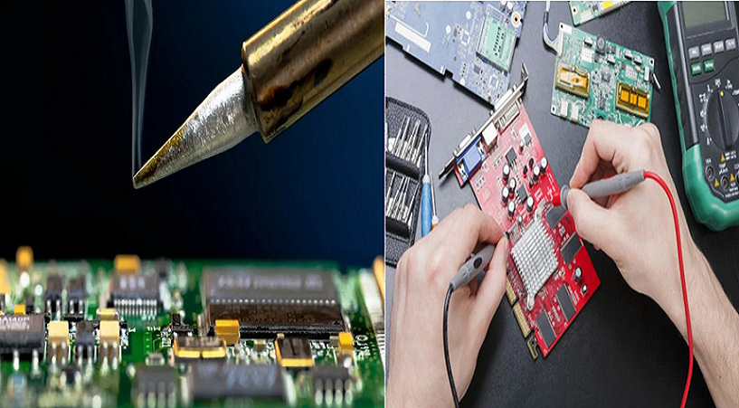
Soldering Iron
Key Features for Electronics Manufacturing
- Temperature control: 325–375°C (617–707°F) range for most PCB soldering; adjustable for lead-free vs. leaded solder
- Tip compatibility: Interchangeable tips (chisel, conical, bevel) to match pad sizes (1:1 tip-to-pad width ratio per IPC-2221)
- ESD safety: Critical for sensitive components in flexible printed circuit and HDI PCB assembly
- Power rating: 30W for prototype circuit board work; 60W+ for high-density interconnect (HDI PCB) with ground planes
Tip Maintenance
- Tin before use: Coat entire tip with thin solder layer to improve heat transfer
- Clean between joints: Wipe with brass sponge to remove oxidation and flux residue
- Retin after use: Reapply solder layer before powering off to prevent corrosion
- Replace when worn: Discard tips with holes, excessive oxidation, or poor heat conduction
Solder
Types & Selection for PCB Prototype
| Solder Type | Composition | Melting Point | Best For | Compliance |
|---|---|---|---|---|
| Leaded | 63Sn/37Pb | 183°C (361°F) | Beginners, prototype circuit board | Non-RoHS |
| Lead-Free | 96.5Sn/3.5Ag | 217°C (423°F) | Electronics manufacturing services, HDI PCB | RoHS |
| Lead-Free | 99.3Sn/0.7Cu | 227°C (441°F) | High-volume electronics manufacturing | RoHS |
Core Specifications
- Gauge: 0.020″–0.032″ (0.5–0.8mm); thinner for small pads on flexible PCB, thicker for large through-holes
- Flux core: Rosin (non-corrosive) for most applications; water-soluble for critical joints (requires post-cleaning)
- Packaging: 15g tubes (prototyping) or 100g spools (electronics manufacturing services)
Safety
- Work in well-ventilated areas to disperse flux fumes
- Wear safety glasses to shield eyes from molten solder and clipped leads
- Use silicone mat to protect workspace from burns and fire hazards
- Keep soldering iron in stand when not in use; avoid contact with skin (tip temperature ≥325°C)
- Wash hands after handling leaded solder to prevent contamination
- Avoid breathing fumes directly; use fume extractor for prolonged electronics manufacturing work
Other
Supplementary Tools for Circuit Board Soldering
- Heat sinks: Clip to sensitive components (diodes, MOSFETs) to prevent heat damage
- PCBite kit: Secures flexible PCB and small prototype circuit boards during soldering
- Compressed air: Dries flux residue after cleaning with IPA
- Needle-nose pliers: Bends component leads and positions small parts
- Multimeter: Tests continuity of solder joints (confirms electrical connection)
Material Compatibility
- Ensure flux is electrically compatible (avoid plumbing flux for electronic manufacturing)
- Match solder type to PCB finish (HASL, ENIG) for optimal wetting
- Use high-temperature PTFE jaws for vises to prevent melting during flexible printed circuit work
Prep
Circuit Board Preparation
- Clean PCB surfaces with 3M Scotch Brite pads to remove tarnish; avoid kitchen-grade pads with cleaners
- Degrease with acetone or methyl hydrate (test on silk screen to prevent ink removal)
- Blow holes clear with compressed air to remove debris
- Inspect for damaged pads or traces (repair before soldering per IPC-6012 standards)
Component Preparation
- Verify component values (resistor color codes, capacitor ratings)
- Bend leads to 45° angles for secure insertion into through-holes
- Trim excessively long leads (leave 1–2mm above PCB surface)
- Clean component leads with IPA to remove oxidation or grease
Soldering Steps
Position Component
- Insert component leads through corresponding PCB holes (bottom side for standard soldering)
- Secure with:
- Bent leads (45° angle) for resistors and diodes
- Masking tape for short-lead components (IC sockets)
- Third hand/PCB vise for flexible PCB or HDI PCB (prevents movement)
- Ensure component is flush with PCB surface (no gaps between component body and board)
Heat the Joint
- Preheat soldering iron to recommended temperature (325°C for leaded, 375°C for lead-free)
- Tin tip with small solder blob to improve heat transfer
- Place tip on both component lead and solder pad simultaneously (use “sweet spot” of tip, not point)
- Hold for 1–2 seconds (longer for large pads/ground planes; avoid exceeding 5 seconds to prevent pad lifting)
Apply Solder
- Touch solder wire to joint (lead + pad interface), not directly to iron tip
- Feed solder until pad is fully coated and forms a concave fillet (volcano shape)
- Use 1–2mm of solder for standard joints; adjust for pad size (larger pads = more solder)
- Stop feeding when flux bubbles and solder flows smoothly around lead
Remove Solder & Iron
- Pull solder wire away first, then remove soldering iron
- Hold component stationary for 2–3 seconds to allow solder to cool and solidify
- Avoid moving joint during cooling (prevents cold joints with dull, grainy appearance)
Inspect
- Visually check joint with magnifying glass:
- Shiny, smooth surface (no dullness or graininess)
- Concave fillet shape (not bulbous or incomplete)
- No solder bridges between adjacent pads
- Full coverage of pad and lead interface
- Test continuity with multimeter (beep = valid electrical connection)
- Trim excess leads with flush cutters (leave 0.5mm above joint)
Tips for Success
- Start with small components (resistors, diodes) before soldering larger parts (capacitors, transformers)
- Install sensitive components (CMOS ICs, MOSFETs) last to minimize heat exposure
- Use flux for lead-free solder to improve wetting (compensates for higher melting point)
- For HDI PCB ground planes: Use larger tip, increase temperature to 400°C, and add extra flux
- Clean flux residue:
- Water-soluble flux: Hot deionized water + brush
- No-clean flux: IPA + lint-free wipe (optional per manufacturer specs)
- Fix common issues:
- Cold joints: Reheat, add small solder, and cool undisturbed
- Solder bridges: Use solder wick to remove excess solder
- Poor flow: Clean pad/lead, increase temperature, or add flux
- Practice on scrap PCB before working on prototype circuit board or flexible printed circuit
Follow IPC-6012 standards for solder joint quality in electronics manufacturing services


![Understanding PCB Costs & Pricing [Your Complete Guide]](https://hdicircuitboard.com/wp-content/uploads/elementor/thumbs/Understanding-PCB-Costs-Pricing-Your-Complete-Guide-qzzhe6mcaxuolkux3xalfktgavumi9y1aqfbs9bpv4.webp "Understanding PCB Costs & Pricing [Your Complete Guide]")


