
Impedance control in HDI PCB design ensures consistent characteristic impedance across transmission lines by optimizing layer stackup, trace geometry, microvia structures, and material properties, complying with IPC‑2221 and IPC‑6012 standards to minimize signal reflection, crosstalk, and attenuation in high‑density hdi pcb manufacturing.
Learn more about: 50Ω / 75Ω / 100Ω Impedance in High Density Interconnect (HDI) PCBs: Design & Production Guide
Key Aspects of HDI Impedance Control
Core Electrical Parameters
Impedance stability relies on quantifiable dimensional and material controls applied throughout hdi pcb fabrication.
- Single‑ended impedance: 50Ω ±5% for standard high‑speed channels
- Differential impedance: 85Ω / 100Ω ±5% for SerDes and differential signaling
- Dielectric constant (Dk): 3.4–3.7, tolerance ±0.05 for consistent impedance
- Dissipation factor (Df): ≤0.009 for low insertion loss at 50GHz
- Impedance deviation: ≤±4% for high‑speed networking applications
Physical Manufacturing Constraints
Factory‑verified limits define achievable impedance consistency in volume production.
- Trace width tolerance: ±8μm after etching
- Dielectric thickness tolerance: ±5μm per layer
- Layer‑to‑layer registration: ±25μm
- Microvia aspect ratio: ≤0.75:1 for reliable plating
- Board warpage: ≤0.2mm/m to preserve impedance uniformity
Learn more about: How to Calculate Impedance for HDI Boards
Layer Stackup Planning for Impedance Stability
Symmetric Stackup Architecture
Symmetric layer sequencing eliminates warpage and maintains balanced impedance across the panel.
- 1+N+1 structure: single build‑up layer per side, 1 lamination cycle
- 2+N+2 structure: dual build‑up layers, 2 cycles, ideal for 56–112Gbps
- Core thickness: 0.4–0.8mm for structural stability
- Build‑up dielectric: 40–75μm for tight reference plane coupling
Reference Plane Placement
Continuous reference planes provide stable return paths and controlled impedance environments.
- Ground planes adjacent to all high‑speed signal layers
- Power‑ground coupling distance: ≤50μm for high decoupling capacitance
- No plane gaps or splits beneath controlled impedance traces
- Dielectric thickness between signal and reference: 50μm nominal
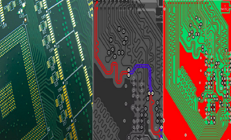
Trace Geometry & Geometry Rules
Trace Width & Spacing Calculations
Trace dimensions directly determine impedance values and are calibrated using field‑solver calculations.
- Inner layer trace/space: 50μm/50μm for advanced designs
- Outer layer trace/space: 75μm/75μm for standard production
- Trace thickness: 12–35μm depending on current and impedance needs
- 3W rule: spacing ≥3× trace width for crosstalk reduction
- Differential pair spacing: fixed to maintain targeted differential impedance
Routing Topology Guidelines
Routing geometry preserves impedance continuity and signal integrity.
- 45‑degree angle routing to eliminate impedance discontinuities
- Minimum bend radius: 3× trace width
- No abrupt neck‑down transitions longer than 200μm
- Length mismatch for differential pairs: ≤200μm
- Parallel routing length limited to minimize crosstalk
BGA Escape Routing with Impedance Control
Fine‑Pitch BGA Fanout Strategies
Escape methods maintain impedance while extracting signals from tight‑pitch components.
- 0.5mm pitch: via‑in‑pad with filled microvias only
- 0.65–0.8mm pitch: hybrid neck‑down and via‑in‑pad
- 1.0mm pitch: dog‑bone fanout acceptable
- Maximum 2 rows escaped per signal layer
- Impedance‑matched neck‑down transitions
Microvia Integration in Escape Paths
Microvia placement eliminates stubs and preserves impedance in BGA fanout.
- Microvia diameter: 75–125μm for BGA escape
- Aspect ratio: ≤0.75:1 for void‑free plating
- Stacked microvias: up to 3 levels for high‑density escape
- Staggered configuration for improved yield and routing space
Microstrip and Stripline Impedance Structures
Microstrip Characteristics (Outer Layers)
Surface‑layer transmission lines with controlled impedance profiles.
- Reference plane: single adjacent ground layer
- Dielectric material: solder mask included in calculations
- Impedance tolerance: ±5% per IPC‑2221
- Typical application: high‑speed external I/O lanes
Stripline Characteristics (Inner Layers)
Embedded transmission lines with superior noise immunity and stability.
- Reference planes: top and bottom ground layers
- Symmetric dielectric environment for consistent impedance
- Reduced crosstalk and EMI radiation
- Preferred for differential pairs and sensitive signals
- Impedance variation ≤±3% in production
Simulation and Modeling for Impedance Accuracy
Field Solver Calculations
Electromagnetic simulation validates impedance before physical fabrication.
- 2D field solvers for standard impedance profiling
- 3D simulation for via transitions and BGA fanout
- Input parameters: Dk, trace width, dielectric thickness, copper roughness
- Output: precise impedance, propagation delay, and loss
PCB Design Tool Integration
Native impedance tools streamline implementation in design flows.
- Altium impedance profile: layer‑specific targets and tolerance setup
- Cadence PCB design: controlled impedance rule sets and constraints
- Impedance calculator integration: real‑time trace adjustment
- Automatic differential pair length matching and spacing
Learn more about: HDI PCB Impedance Control: Design, Manufacturing & Performance Guide
Fabrication Validation & Quality Control
TDR Impedance Testing
Time‑domain reflectometry verifies impedance across production panels.
- 100% TDR testing for high‑speed hdi pcb manufacturing
- Test coupons included on every production panel
- Measurement range: DC to 50GHz
- Automated reporting per IPC‑TM‑650 standards
Cross‑Section Analysis
Physical inspection validates dielectric and trace geometry compliance.
- Dielectric thickness measurement: ±5μm accuracy
- Trace width and sidewall profile inspection
- Microvia plating integrity and annular ring check
- Impedance correlation to dimensional parameters
Best Practices for HDI Impedance Control
Engage Manufacturers Early
Early collaboration aligns design with factory capabilities and material availability.
- Pre‑design stackup review with hdi pcb manufacturer
- Material selection based on in‑stock dielectric laminates
- Process capability validation for fine lines and microvias
- Impedance target alignment with production tolerances
Manage Vias & Continuity
Via management eliminates parasitic effects that disrupt impedance.
- Blind and buried microvias to eliminate stubs
- Via stub length: ≤20μm for high‑speed signals
- Ground stitching vias at ≤1mm intervals for shielding
- Avoid via placement within differential pair gaps
Keep Trace Lengths Short
Short traces reduce loss and simplify impedance matching.
- Critical high‑speed trace length: ≤50mm
- Impedance‑controlled sections kept direct and unbroken
- Minimize layer transitions for impedance‑critical nets
- SerDes lanes routed with direct, shortest paths
Comparative Tables
Microstrip vs Stripline Impedance Performance
| Structure | Layer Location | Impedance Stability | EMI Performance |
|---|---|---|---|
| Microstrip | Outer Layers | Good | Moderate |
| Stripline | Inner Layers | Excellent | Excellent |
BGA Pitch vs Impedance‑Compatible Fanout
| BGA Pitch | Fanout Type | Impedance Stability |
|---|---|---|
| 0.5mm | Via‑in‑Pad | Excellent |
| 0.65–0.8mm | Hybrid Neck‑Down | Good |
| 1.0mm | Dog‑Bone | Moderate |
Learn more about : BGA Routing in HDI PCBs: Fanout & Escape Techniques
Core Technical Specifications
- Layer count: 4–40 layers
- Board thickness: 0.40–7.60mm
- Minimum microvia diameter: 75μm
- Aspect ratio: ≤0.75:1
- Trace/space: 50μm/50μm (inner); 75μm/75μm (outer)
- Impedance tolerance: ±5%
- Dielectric thickness: 40–75μm
- Registration accuracy: ±25μm
- Warpage limit: ≤0.2mm/m
Case Study
Project Overview
Board type: 12‑layer 2+8+2 HDI PCB; Application: 800G optical transceiver; Impedance target: 100Ω differential ±5%; BGA pitch: 0.65mm.
Issues Encountered
Initial asymmetric stackup caused 0.27mm/m warpage; microvia aspect ratio 1.1:1 created plating voids; 90‑degree bends induced impedance discontinuities; trace spacing insufficient for crosstalk and impedance targets.
Corrective Actions
Implemented fully symmetric stackup; reduced microvia aspect ratio to 0.7:1; applied 45‑degree routing; optimized trace width and spacing per field‑solver results; switched to low‑loss dielectric material.
Final Results
Impedance held to ±4.1% tolerance; warpage stabilized at 0.16mm/m; insertion loss ≤0.58dB at 50GHz; production yield improved from 79% to 96.3%; full compliance with IPC‑6012 Class 3.
Common Design Errors
- Asymmetric stackups induce warpage exceeding 0.25mm/m and break impedance consistency.
- Microvia aspect ratio >0.75:1 causes plating voids and parasitic impedance shifts.
- Reference plane gaps under controlled impedance traces disrupt return paths and increase signal reflection.
- 90‑degree trace angles create impedance discontinuities and degrade signal eye diagrams.
- Failure to calibrate trace width to dielectric thickness results in impedance drift beyond tolerance.
Frequently Asked Questions
Q1: What impedance tolerance is standard for high-speed HDI PCBs?
A1: Industry and IPC standards require ±5% tolerance for single‑ended and differential impedance in high‑speed hdi pcb fabrication.
Q2: Which stackup structure provides the best impedance stability?
A2: Symmetric 2+N+2 HDI stackups deliver optimal impedance stability and warpage control for 56–112Gbps applications.
Q3: How are impedance values calculated in HDI design?
A3: Values are calculated using 2D field solvers with trace geometry, dielectric thickness, Dk, and copper roughness inputs.
Q4: What fanout method supports impedance for 0.5mm BGA pitch?
A4: Via‑in‑pad with copper‑filled microvias is the only production‑ready method for impedance‑controlled 0.5mm pitch BGA escape.
If you need professional HDI PCB design support or quotation, our team provides free DFM check and fast turnaround.


![Understanding PCB Costs & Pricing [Your Complete Guide]](https://hdicircuitboard.com/wp-content/uploads/elementor/thumbs/Understanding-PCB-Costs-Pricing-Your-Complete-Guide-qzzhe6mcaxuolkux3xalfktgavumi9y1aqfbs9bpv4.webp "Understanding PCB Costs & Pricing [Your Complete Guide]")


