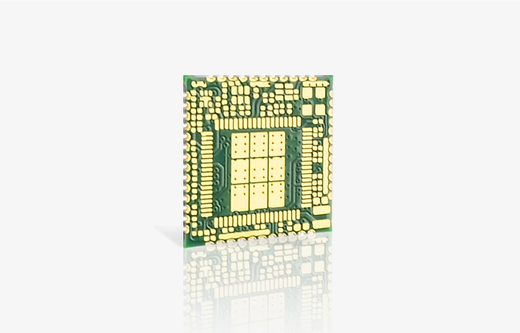
- Blind vias, buried vias, Ultra HDI PCB
- High frequency low loss PCB material
- Low loss high speed PCB materials
- R-5775, R-5785, R-5795, TU-872 SLK , TU-872 SLK SP, TU 933+, I-Tera MT40, Astra MT77, Tachyon 100G material
- EM-888, EM-888(S), EM-888(K), EM-526, EM-528, EM-528K, IT-968, IT-968 SE, IT-988G, IT-988G SE material
Microvia PCB Solutions | Blind & Buried Vias Filling & Plating Technologies
Microvia Basics & Size Grading
What is Microvia in PCB Manufacturing
A microvia is a laser-drilled conductive aperture with a maximum diameter of 0.2mm, engineered for connecting 1–2 adjacent layers on microvia PCBs. Unlike conventional through-holes or HDI’s multi-layer interconnect vias, our microvia PCB manufacturing processes prioritize filling and plating integrity over overall board density. Each microvia is precision-machined into a conical frustum shape, a design that enhances both electrical conductivity and mechanical stability. Distinct from HDI microvias— which are optimized for high-layer count connectivity— standalone microvia PCBs serve as a precision upgrade for standard PCB architectures, elevating reliability in compact, low-layer electronic devices.
Microvia Size Grades & Application
We have developed a proprietary three-tier size classification system for microvia PCBs, a framework that diverges from HDI’s layer-centric categorization and is tailored to targeted application scenarios:
- Ultra-mini microvia (0.08–0.1mm): Engineered for buried via PCBs used in medical implant devices. These microvias utilize biocompatible epoxy filling and lead-free plating to meet stringent FDA sterility requirements, with a maximum aspect ratio of 0.8:1 to prevent structural fracture under physiological stress.
- Standard microvia (0.1–0.15mm): Deployed in blind via PCBs for 5G sensor modules. Produced with laser-drilling precision of ±3μm and copper filling, this grade supports a 5A current capacity while cutting signal loss by 20% compared to traditional via technologies.
- Large-caliber microvia (0.15–0.2mm): Integrated into blind and buried via boards for automotive ADAS power layers. Leveraging resin-copper hybrid filling, this microvia type balances high thermal dissipation efficiency with robust structural strength, ideal for high-power automotive electronics.
Blind & Buried Vias Core Processes
Microvia Filling Material Options
Our blind/buried vias and standalone microvias utilize three specialized filling material formulations, a portfolio that sets itself apart from HDI’s generic filling solutions:
- Pure copper filling: Designed for blind via PCBs in aerospace equipment. Manufactured with vacuum pulse plating technology to eliminate internal voids, this filling material delivers 10 times the thermal conductivity of epoxy alternatives and supports continuous current loads of up to 8A.
- Epoxy-copper resin filling: Optimized for buried via PCBs in consumer electronics. This cost-effective blend reduces filling expenses by 30% relative to pure copper, while still maintaining a 3A current capacity and sufficient thermal dissipation for everyday use cases.
- Biocompatible epoxy filling: Crafted for ultra-mini blind and buried vias in implantable medical devices. Compliant with USP Class VI standards and free of heavy metal contaminants, this material ensures zero tissue irritation, a critical requirement for long-term in vivo applications.
Blind/Buried Vias Plating Standards
We enforce two customized plating standards exclusively for blind and buried vias, a set of specifications tailored to microvia performance rather than HDI’s board-level quality benchmarks:
- Void-free electroless plating: Mandated for blind via PCBs featuring in-pad via designs. This standard requires plating thickness uniformity within ≤5μm and zero voids confirmed by 100% X-ray inspection— a non-negotiable requirement for fine-pitch BGA assembly with 0.2mm pitch or smaller.
- CTE-matched pulse plating: Specified for buried via PCBs in high-temperature automotive devices. The plating is engineered to match the laminate’s coefficient of thermal expansion (CTE) at 16ppm/°C, preventing thermal fracture during extreme temperature cycling (-40°C to 125°C) and backed by a 1000-cycle reliability guarantee.
Stacked vs Staggered Microvias
Stacked Microvias for Space-Saving
Our stacked microvia technology— distinct from HDI’s stacked layer architectures— involves vertically aligning copper-filled blind or buried vias. This design reduces board surface area by 40% for blind via PCBs in smart wearables, where space efficiency is paramount. The manufacturing process requires a 2μm copper cap to be pre-plated on inner vias, preventing inter-layer detachment. Unlike HDI’s 8+ layer stacking capabilities, our solution prioritizes compactness over layer count, with a maximum stack height of 3 layers.
Staggered Microvias for Signal Integrity
Our staggered microvias— differing from HDI’s staggered layer layouts— are offset on adjacent layers by a distance of at least 1x the via diameter. This configuration eliminates signal crosstalk, making it ideal for buried via PCBs in high-frequency industrial sensors operating at 24GHz or higher. Unlike stacked microvias, staggered variants do not require copper filling for inner vias, cutting production costs by 15%. Additionally, they maintain a 50Ω impedance tolerance of ±2%, ensuring stable signal transmission in high-speed applications.
Microvia PCB Non-HDI Application Cases
Industrial Control Blind Via PCB Upgrade Case
We completed a targeted upgrade of a standard 4-layer industrial control PCB to a blind via PCB— without converting to HDI architecture— by replacing traditional through-holes with 0.12mm blind vias filled with epoxy-copper resin. The upgrade reduced the board footprint by 25%, achieved IP65 moisture resistance compliance, and lowered assembly defect rates by 30%— a critical improvement for factory floor equipment exposed to harsh environments. Notably, the modification only increased costs by 10%, delivering a 60% cost saving compared to a full HDI conversion.
Automotive Buried Via PCB Retrofit Case
We retrofitted a 6-layer automotive BMS PCB to a buried via PCB (without implementing HDI stackup) by integrating 0.15mm buried vias with CTE-matched plating for power layer connections. The retrofit boosted thermal dissipation efficiency by 35% and passed 1000-hour thermal cycling tests, fully meeting AEC-Q200 automotive electronics standards. By avoiding the high-layer complexity of HDI technology, this solution provides a cost-effective alternative for mid-range EVs with tight budget constraints.
Microvias PCB Via Structures
High density interconnects are categorized by six design types in IPC-2226. They are grouped by stackup characteristics in the following categories: Type I, Type II, Type III, Type IV, Type V, and Type VI
TYPE I
1 [C] 0 or 1 [C] 1, with through-vias from surface to surface.
TYPE II
1 [C] 0 or 1 [C] 1, with buried vias in the core and may have through-vias connecting the outer layers from surface to surface.
TYPE III
2 [C] 0, two or more HDI layers added to through-vias in the core or from surface to surface.
TYPE IV
1[P] 0 where P is a passive substrate with no electrical connecting functions.
TYPE V
Coreless constructions using layer pairs.
TYPE VI
Alternate constructions of coreless construction using layer pairs.
Blind Microvias
Blind microvias start in the surface layer and terminate 1 layer below the surface, although they could terminate or 2 layers below the surface layer if the aspect ratio is kept low. If you need to span 2 layers, it’s better to use stacked microvias (see below) or staggered microvias as these will be more reliable. Blind microvias could be filled or unfilled.
Buried Microvias
Buried microvias have basically the same structure as blind vias and span between two interior layers and do not reach either circuit board surface. Just like blind microvias, it’s best the aspect ratio stays low and they span a single layer to ensure reliability and ease of fabrication. These vias are filled with copper, either using a plating process with pure copper or with a epoxy + copper resin to ensure a strong connection across the head of the microvia. It’s important that the process being used for plating results in void-free structures to ensure maximum reliability.
Stacked or staggered vias
Stacked microvias create more space for the high-density wiring and fanout from low-pitch BGAs but it increases the PCB cost. Stacked microvias should only be used when the design doesn´t have sufficient space to use staggered vias. Microvias stacked on buried vias require additional Cu cap plating process for the buried vias and microvias stacked on microvias require additional Cu filling of the inner layer microvias.
As the layer-by-layer process for forming low aspect ratio microvias makes them useful in stacked applications. Stacked microvias are simply stacks of buried vias, or a blind microvia stacked on top of buried microvias. This is the standard way to span between multiple layers in an HDI PCB. The internal buried microvias in the stack need to be filled with conductive paste and plated over to ensure strong contact as the next via in the stack is deposited and plated. The alternative to stacked microvias is staggered microvias, where microvias on successive layers are offset from each other.
HDI Microvia Fabrication
Depending on the size of the vias, they can be mechanically drilled and plated (followed by stacking and pressing each layer), or they can be formed with a high-power laser. The latter process is constantly being improved and is preferred in high volume PCB manufacturing thanks to its high throughput. New advances in laser drilling techniques are pushing microvia sizes down to as small as 15 µm.
After drilling and cleaning, the via hole is plated, either with a sputtering process, electrolytic deposition, or electroless copper plating process. The goal in the plating process is to prevent the formation of voids, dimples, bumps, or any other structural defect in the filled via. Voids are also a reliability concern as stress can concentrate around the edge of the void where copper is thinner if stress is applied to the via structure.
During fabrication, laser-drilled microvias have a lower potential for manufacturing defects than normal vias. Mechanically-drilled microvias can have defects due to drill vibration as the drill wears out, and mechanical microvia drilling is only useful down to 6 to 8 mil diameters, depending on the fabricator’s tooling .
Filled or Unfilled Microvias
It is possible to either fill microvias with copper or leave them unfilled. For buried microvias, it is necessary to fill the via hole with copper, especially if they are to be stacked. Any voids present in the interior of the via barrel can lead to premature fracture during reflow. Although it is possible to leave blind microvias unfilled, in-pad blind microvias must always be filled.
Following the filling, the manufacturer will plate the microvia. They typically use epoxy and copper resin or pure copper for the process. Beginning with a conformal coating, the manufacturer typically uses pulse plating to fill in the body of the microvia with solid copper, thereby eliminating voids. Additives in the filler material are necessary during the plating process, as their absence may result in void formation. Another reason for using additives is to prevent the copper from being concentrated on the walls and the top surface of the microvia. Uneven deposition of copper along the via body may also be conformal plating, and this may lead to the formation of voids.
Via Filling Options
As a refresher, a via is a copper plated hole that is used to connect two or more layers within a PCB together. Via Fill is a special PCB manufacturing technique used to selectively and completely close via holes with epoxy. There are many instances in which a PCB designer might want to have a via filled. Some key benefits are:
Via In Pad
Perhaps one of the greatest benefits of via fill is the option to implement via in pad.This process is becoming more and more popular and preferred as opposed to using the traditional “dog bone” method to transfer signal from the BGA, through the via, and on to inner layers. In this process, also known as active pad, vias are filled, planarized, plated over with copper. While the Via-In-Pad process does increase cost there can be significant benefits over conventional through hole technology.
Some key benefits are:
- Tighter BGA pitches
- Increased thermal dissipation
- Reduced layer count or board size, which ultimately may reduce cost
- Improved routing density (higher density per layer)
- Strengthening Pad attachment
- Gives high frequency designs the shortest possible route to bypass capacitors
- Overcomes high speed desogn issues and constraints such as low inductance
Conductive Via Filling
Conductive via filling allows the effective transfer of electrical signals from one side of the circuit board to the other, while enhancing its thermal transfer properties of the via. Conductive filled vias (copper or silver are the most common) are especially helpful for conducting a large amount of heat away from components as the metallic nature of the fill wicks heat away from the IC.
Silver epoxy is more cost-effective and used more frequently but copper conductive epoxy is far better in terms of thermal conductivity. However, both will improve the quality of current conduction between the vias and the PCBs internal layers. It should be noted that conductive fill of vias is approximately 5x the cost of non-conductive fill.
Non-Conductive Via Filling
Non-conductive via fill is done using the same process as conductive except that it is usually done to prevent solder or other contaminants from entering the via rather than conducting heat and a signal. It also provides structural support for a copper pad covering the hole in the case of a via-in-pad. Keep in mind that the vias are still plated with copper so they will conduct heat and electrical signals, as the only difference between traditional vias is the air in the space is replaced by the fill material.
It is always recommended to match the CTE values of the via filling to be used with the surrounding laminate to avoid future stress fractures due to contraction or expansion. Because the via fill material will heat up and expand far more rapidly than the laminate, this unequal expansion can cause a fracture to appear between the pad and the hole wall.
Copper-Plated Shut Filled Vias
Most PCB designers have experience with the use of filled vias using epoxy, but many are not familiar with the process of copper plated shut for either through vias and/or microvias, as not all PCB fabricators have invested in the proper equipment to perform this process.
Benchuang Electronics has developed a process that allows us to plate shut through-hole vias, up to 12 mils in diameter, without concern of voids, air pockets, or fluid entrapment in the holes. Without question, plated shut vias provide 10X the thermal conductivity of any other via fill solution, which makes it the most logical choice for thermal dissipation.
Generally speaking, when the aspect ratio gets to 10:1 or via diameter is less than 8 mils, that is where we would opt to copper plate shut a via, but there are other specific attributes where it is very difficult to fill, or plate shut vias:
- Thin materials or subs (less than 20 mils) are more difficult to process through planarization as the material can tear and/or distort.
- If wrap plating is required, so terminating surfaces have a buildup of copper, making fine lines/spaces more difficult to process.
- PTFE/Teflon materials will dramatically distort.
Staggered Microvias
Like stacked vias, staggered vias also connect different layers of the board. However, they are never in direct contact with each other as their drill axes are separate, which offsets their position on adjacent layers.
Staggering the microvias involves fewer design steps. Because the drilled hole is not directly above the one below it, laser-drilled staggered vias do not need copper filling. This makes the design less complicated.
While designing a staggered via structure, the spacing between the laser-drilled holes is the primary concern. The possibility of the staggered via design depends on the vertical distance between the centers of two adjacent microvias. A viable staggered design requires the vertical separation to be more than the diameter of the microvia.
Stacking microvias exerts pressure on the via walls. The pressure can detach the topmost via from its pad. Therefore, designers prefer a staggered microvia configuration when they have to interconnect more than two layers.
However, if the design has space constraints, staggered vias may not be the right choice. Although less complex, staggering makes them use up more space on the board. On the other hand, staggering has negligible crosstalk issues because of the offset. Staggering introduces more discontinuity in the signal path. This makes it difficult to maintain a uniform via impedance requirement in a high-speed design.
Stacked Microvias
Stacked vias have the vias placed directly one atop the other. The operator drills each via and plates it before stacking it above another to connect various layers. They use two narrow annular rings, one on the top and the other, on the bottom. The upper annular ring helps in precise registration, while the bottom one makes the electrical connection.
The operator fills the stacked vias with electroplated copper. This not only provides structured support but also ensures a solid electrical connection. However, improper deposition can create defects like voids and inferior bonding between the base of the via and the target pad beneath it, hampering the reliability of the stacked vias.
While compactness is the primary advantage of stacked vias, in HDI boards stacked vias also ensure flexibility during practical routing. In addition, stacked vias help maintain properly controlled impedance of the signal from its source to its destination.
Exerting pressure from the z-axis of the dielectric on the microvia actually impacts the reliability. The reason for this is a mismatch in the CTE of the materials. For instance, consider the situation beyond the glass transition temperature. While copper expands only up to 16 parts per million, the dielectric expands nearly 200 parts per million.
As long as only a single layer is present, there is not much of an issue. The discrepancy really begins when the layer number increases to two and beyond. For instance, with a layer count of three or more, the mismatch crosses tolerance limits. It can lead to microvia failure due to its barrel or its corner cracking up. This led to designers staggering the vias rather than stacking them vertically.
Get started with Microvia PCB
- Blind vias, buried vias, Ultra HDI PCB
- High frequency low loss PCB material
- Low loss high speed PCB materials
- R-5775, R-5785, R-5795, TU-872 SLK , TU-872 SLK SP, TU 933+, I-Tera MT40, Astra MT77, Tachyon 100G material
- EM-888, EM-888(S), EM-888(K), EM-526, EM-528, EM-528K, IT-968, IT-968 SE, IT-988G, IT-988G SE material