
What Are the Minimum Trace Width, Spacing, and Microvia Size for HDI PCB Mass Production?
High density interconnect (HDI) PCBs rely on precise trace and microvia dimensions to balance manufacturing feasibility, performance, and cost in mass production. The minimum trace width, spacing, and microvia size are defined by industry standards (IPC-2221, IPC-2226, IPC-6012), material capabilities, and production yield requirements. For electronic engineers, PCB procurement teams, and electronics enthusiasts, understanding these thresholds is critical to avoiding fabrication delays, excessive scrap, and performance failures. This guide breaks down the minimum dimensions for conventional and HDI PCBs, key constraints, and practical tradeoffs for volume production.
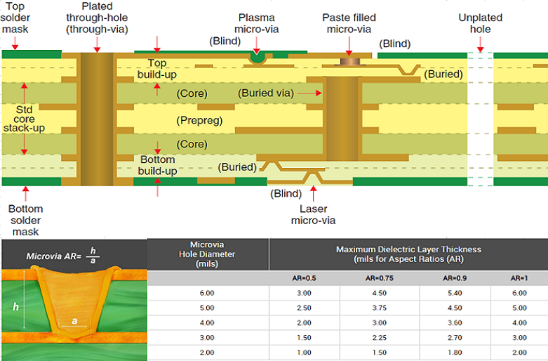
Learn more about: How to Design HDI Microvia PCB
Trace Width & Spacing – Core Parameters for Conductivity
Trace width and spacing directly impact current carrying capacity, signal integrity, and manufacturing yield. Minimum values vary by PCB type (conventional vs. HDI) and copper weight, with strict adherence to IPC standards to ensure reliability in mass production.
Conventional PCB (Non-HDI)
Conventional PCBs use through-hole vias and thicker traces, with minimum dimensions optimized for standard fabrication processes.
- Minimum trace width:
- 3mil (75μm) for 1oz copper (standard for signal traces) per IPC-2221 Class 2.
- 4mil (100μm) for 2oz copper (power traces) to accommodate higher current.
- 6mil (150μm) for 3oz copper (high-power applications like industrial controllers).
- Minimum spacing:
- 3mil (75μm) between adjacent traces (IPC-2221 Class 2) for low-voltage signals (<30V).
- 4mil (100μm) for high-voltage signals (>30V) to prevent arcing.
- 5mil (125μm) for inner layers with 2oz+ copper to account for etching variability.
- Key standards & tradeoffs:
- IPC-2221 specifies trace width calculations based on current: 1oz copper trace with 3mil width carries ~0.5A without excessive heating.
- Reducing width below 3mil increases etching defects by 15–20% in mass production, raising scrap rates and cost.
HDI PCB (1+N+1 Stackup)
Entry-level HDI (1+N+1) uses single build-up layers, enabling finer traces while maintaining high yields.
- Minimum trace width:
- 2mil (50μm) for 0.5oz low-profile copper (outer layers) with laser direct imaging (LDI).
- 2.5mil (62.5μm) for 1oz copper (inner layers) to ensure consistent plating.
- Minimum spacing:
- 2mil (50μm) between traces (IPC-2226 Class 2) for standard density.
- 1.5mil (37.5μm) achievable with advanced LDI, but adds 10% cost premium due to tighter process control.
- Key standards & tradeoffs:
- IPC-2226 requires trace spacing to match width for HDI to minimize crosstalk.
- 2mil trace/space supports 0.4mm pitch BGAs, replacing 6-layer conventional PCBs with 4-layer HDI.
HDI PCB (2+N+2/Any-Layer)
Advanced HDI (2+N+2/any-layer) uses stacked or staggered microvias and ultra-fine traces for high-density designs.
- Minimum trace width:
- 1mil (25μm) for 0.33oz ultra-thin copper (any-layer HDI) with modified semi-additive processing (mSAP).
- 1.5mil (37.5μm) for 0.5oz copper (2+N+2 stackup) for reliable mass production.
- Minimum spacing:
- 1mil (25μm) between traces (IPC-2226 Class 3) for critical high-speed signals.
- 1.2mil (30μm) for inner layers to balance density and yield.
- Key standards & tradeoffs:
- mSAP process enables 1mil traces but increases material cost by 20–30% compared to subtractive etching.
- IPC-6012 Class 3 mandates 1mil trace/space for aerospace and medical HDI applications.
Microvia Size – Precision for Layer Interconnection
Microvias are laser-drilled holes that enable layer-to-layer connectivity in HDI PCBs. Minimum size is governed by aspect ratio, plating reliability, and laser drilling capabilities.
Standard HDI Mass Production
Standard HDI (1+N+1/2+N+2) uses microvias for moderate density, with dimensions optimized for high yields.
- Minimum microvia diameter:
- 75μm (3mil) for 1+N+1 stackup, with aspect ratio ≤0.8:1 (depth ≤60μm) per IPC-6016.
- 80μm (3.2mil) recommended for mass production to achieve 85–90% yield.
- Depth & plating requirements:
- Maximum depth of 75μm for 75μm diameter to ensure uniform copper plating (minimum 12μm thickness).
- Unfilled microvias acceptable for 1+N+1; stacked microvias in 2+N+2 require 100% copper filling.
- Key standards & tradeoffs:
- IPC-T-50M defines microvias as blind holes with ≤1:1 aspect ratio and depth ≤0.25mm.
- 75μm microvias reduce board area by 30% compared to 100μm microvias, enabling finer component placement.
High-Density HDI (Any-Layer)
Any-layer HDI demands ultra-small microvias for extreme density, with tighter process controls.
- Minimum microvia diameter:
- 50μm (2mil) for any-layer stackup, aspect ratio ≤0.6:1 (depth ≤30μm).
- 60μm (2.4mil) for volume production to mitigate plating voids.
- Special requirements:
- Laser drilling with UV lasers for clean hole walls; CO2 lasers unsuitable for diameters <60μm.
- Copper-filled and planarized for via-in-pad (VIP) applications, supporting 0.2mm pitch BGAs.
- Key standards & tradeoffs:
- Yield drops to 70–75% for 50μm microvias due to increased drilling and plating complexity.
- IPC-2226 requires target pad diameter ≥80% of microvia diameter to reduce stress concentration.
Key Mass Production Constraints
Minimum trace width, spacing, and microvia size are not arbitrary—they are limited by manufacturing realities, material capabilities, and cost tradeoffs.
Yield Impact
- Trace or spacing below 2mil or microvias smaller than 75μm reduce production yield by 10–20% per 0.5mil or 12.5μm reduction.
- Example: 1mil traces vs. 2mil traces increase scrap rates from 5% to 15% in 100k-unit runs.
- Quality control measures: Automated optical inspection (AOI) and X-ray inspection for microvia plating integrity; 100% electrical testing for open or short circuits.
Material Limits
- Dielectric materials:
- Standard FR-4 supports down to 2mil traces; low-loss laminates enable 1mil but cost twice as much.
- Prepreg thickness ≥60μm for 75μm microvias to prevent drill-through damage.
- Copper weight:
- Thin copper (0.33–0.5oz) required for traces below 2mil; thick copper (2oz+) limits minimum trace width to 3mil or larger.
- Key comparisons:
- FR-4 provides lower cost but restricts minimum trace width to 2mil, while low-loss materials support 1mil at a premium.
- 0.5oz copper enables 2mil traces but carries 20% less current than 1oz copper.
Equipment Requirements
- Laser drilling: UV lasers required for microvias smaller than 100μm; CO2 lasers suitable for 100μm or larger.
- Imaging: LDI required for traces below 2mil; conventional photolithography limited to 3mil or larger.
- Plating: Vertical continuous plating (VCP) systems for uniform copper deposition in microvias smaller than 75μm.
- Cost impacts:
- LDI equipment increases setup cost by 15–20% but enables 2mil traces instead of 3mil.
- UV laser drilling is 30% slower than CO2 drilling, increasing per-unit cost for 50μm microvias.
Cost Tradeoffs
- Every 0.5mil reduction in trace width adds 5–8% to per-unit PCB cost in mass production (100k+ units).
- 50μm microvias cost 40–50% more than 75μm microvias due to slower drilling and higher yield loss.
- Example: A 10-layer 2+N+2 HDI with 2mil traces and 75μm microvias costs 15% less than the same board with 1mil traces and 50μm microvias.
Comparative Table – Minimum Dimensions by PCB Type
| Parameter | Conventional PCB | HDI (1+N+1) | HDI (2+N+2/Any-Layer) |
|---|---|---|---|
| Minimum Trace Width (1oz copper) | 3mil (75μm) | 2mil (50μm) | 1mil (25μm) |
| Minimum Spacing (1oz copper) | 3mil (75μm) | 2mil (50μm) | 1mil (25μm) |
| Minimum Microvia Diameter | N/A | 75μm (3mil) | 50μm (2mil) |
| Aspect Ratio Limit | N/A | ≤0.8:1 | ≤0.6:1 |
| Production Yield | 90–95% | 85–90% | 70–85% |
| IPC Standard | IPC-2221 Class 2 | IPC-2226 Class 2 | IPC-2226 Class 3 |
| Copper Weight Range | 1–4oz | 0.5–2oz | 0.33–1oz |
Long-Tail Considerations & FAQ
How Copper Weight Affects Minimum Dimensions
- Copper weight directly correlates with trace width: 0.5oz copper allows 2mil traces, while 2oz copper requires 3mil or larger traces to avoid overheating.
- Example: A 3mil trace with 1oz copper carries 0.5A; the same trace with 2oz copper carries 0.8A, but requires 4mil spacing.
PCB vs. PCA – Assembly Impact of Minimum Dimensions
- Conventional PCB: 3mil traces compatible with standard SMT assembly; no incremental cost.
- HDI (1+N+1): 2mil traces require fine-pitch placement (±0.05mm accuracy); assembly cost increased by 10%.
- HDI (any-layer): 1mil traces and 50μm microvias need flip-chip assembly; assembly cost increased by 20–30%.
How to Validate Minimum Dimensions for Mass Production
- Conduct DFM (Design for Manufacturability) review with HDI manufacturers to align with their equipment capabilities.
- Test with prototype runs: Produce 50–100 units to measure yield and performance before scaling to 10k+ units.
- Reference IPC test methods (IPC-TM-650 2.6.27) to verify trace conductivity and microvia reliability.
Conclusion
The minimum trace width, spacing, and microvia size for HDI PCB mass production are defined by a balance of IPC standards, manufacturing capabilities, and cost-efficiency. Conventional PCBs rely on 3mil traces or spacing and through-hole vias for high yields, while standard HDI (1+N+1) uses 2mil traces and 75μm microvias to save space. Advanced any-layer HDI pushes to 1mil traces and 50μm microvias for extreme density but requires premium processes and materials. By aligning designs with these thresholds, teams avoid fabrication delays, reduce scrap, and ensure consistent performance in volume production. Early collaboration with HDI manufacturers, adherence to IPC standards, and prototype validation are key to translating minimum dimensions into reliable, cost-effective products—whether for consumer electronics, automotive systems, or medical devices.


