- Blind vias, buried vias, Ultra HDI PCB
- High frequency low loss PCB material
- Low loss high speed PCB materials
- R-5775, R-5785, R-5795, TU-872 SLK , TU-872 SLK SP, TU 933+, I-Tera MT40, Astra MT77, Tachyon 100G material
- EM-888, EM-888(S), EM-888(K), EM-526, EM-528, EM-528K, IT-968, IT-968 SE, IT-988G, IT-988G SE material
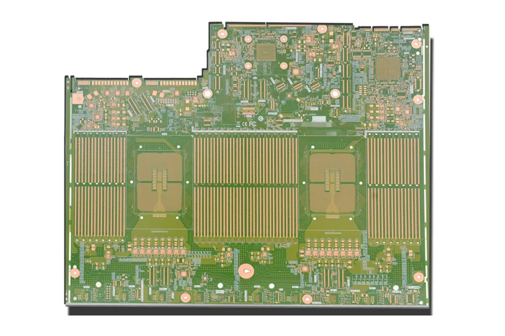
Custom Multilayer PCB Solutions | High layer count PCB Board for Industrial & Automotive Applications
Layer-Customized Multilayer PCB for Targeted Industry Needs
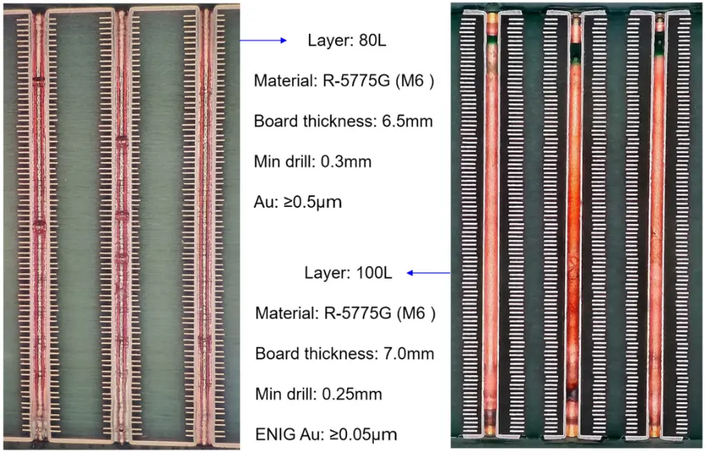
Industrial Control 4/6 Layer PCB Engineering Specifications
Our 4-layer and 6-layer PCBs engineered for industrial control systems are built to withstand the harsh operational conditions of factory floors—far exceeding generic manufacturing benchmarks. The 4-layer PCB leverages high-Tg FR-4 material with a glass transition temperature of ≥170°C, enabling stable performance across a -40°C to 85°C temperature range. Equipped with 3/3mil line width and spacing, plus 0.2mm via diameters, this board supports 24V industrial power inputs while incorporating dedicated anti-interference shielding between signal and power layers. For complex programmable logic controllers (PLCs), the 6-layer variant adds an independent ground plane, cutting electromagnetic interference (EMI) by 30% compared to 4-layer designs. It integrates 0.15mm blind vias to eliminate signal crosstalk from through-holes, with full compliance to IEC 61010 industrial safety standards for hazardous electrical equipment.
Automotive BMS 8/12 Layer PCB Custom Solutions
Our 8-layer and 12-layer PCBs designed for automotive battery management systems (BMS) are fully optimized to meet AEC-Q200 automotive electronics qualification standards, with bespoke thermal and electrical enhancements. The 8-layer PCB adopts a symmetric stackup structure (signal-ground-power-ground-signal) to minimize warpage to ≤0.5%—a 50% improvement over the industry average of 1.0%—during prolonged operation in high-temperature engine bays. Its 2/2mil line width and spacing accommodate high-density cell monitoring circuits for EV battery packs. The 12-layer version integrates two dedicated thermal dissipation planes and 3mm×3mm copper coin reinforcement for 100A high-current pathways, a critical feature for BMS supporting 100kWh+ battery configurations. Every unit is backed by a 1000-hour thermal cycling reliability guarantee, ensuring durability in extreme automotive environments.
High-Layer PCB (10–16 Layers) Custom Fabrication & Rigorous Testing Protocols
10/12 Layer PCB Custom Stackup Design Services
As a specialized manufacturer of 10-layer PCBs, our custom stackup design service addresses the core challenge of misaligned layer functionality in high-complexity electronic devices. For aerospace navigation systems, we engineer 12-layer PCBs with a symmetric “RF-signal-ground-power-ground-signal-RF” stackup, delivering ±2% impedance control at 50Ω for 24GHz satellite communication signals. The design combines Rogers 4350B material for RF layers (to ensure high-frequency performance) and high-Tg FR-4 for power layers (to optimize cost-efficiency). For high-performance industrial servers, the 10-layer PCB uses an asymmetric “signal-power-ground-signal” stackup to support 10Gbps data transmission speeds. It incorporates precision back-drilling to eliminate stub noise in high-speed signal channels, preventing signal degradation in bandwidth-intensive applications.
16 Layer PCB Reliability Testing Protocols
Our 16-layer PCB—our highest-tier customized layer option—undergoes a proprietary 7-step reliability testing regimen, far surpassing basic industry inspection standards for high-complexity projects:
- X-ray void inspection: Verifies buried via void rates ≤0.5% to ensure electrical connectivity;
- Extreme thermal cycling: Exposes boards to -55°C to 125°C for 2000 cycles to simulate aerospace/automotive temperature stress;
- Vibration durability testing: Subjects units to 20G force across 10–2000Hz frequencies, tailored to aerospace deployment requirements;
- Humidity resistance testing: Sustains exposure to 85% relative humidity at 85°C for 1000 hours to validate moisture tolerance;
- High-frequency impedance testing: Ensures ±3% impedance accuracy across all high-speed layers;
- Solderability validation: Complies with IPC-J-STD-002 standards to guarantee robust solder joint formation;
- 100% electrical continuity testing: Uses flying probe technology to detect micro-scale open circuits or short circuits.
Every 16-layer PCB shipment includes a comprehensive compliance report, fully suitable for regulatory submissions in aerospace and defense sectors.
Custom Multilayer PCB Non-Standard Project Success Cases
Industrial 6 Layer PCB Custom Modification Case Study
A leading industrial robot original equipment manufacturer (OEM) partnered with us to resolve critical dust-proof and anti-static flaws in their standard 6-layer control board, a problem their previous supplier failed to address. Our engineering team delivered three key custom modifications to the 6-layer PCB:
- Applied a 0.2mm thick solder mask overcoat to achieve IP65 dust resistance ratings;
- Coated outer layers with a carbon-film anti-static treatment, achieving a surface resistance range of 10⁶–10⁹Ω to dissipate static charges;
- Redesigned via placement layouts to eliminate static charge accumulation hotspots.
The modified board passed 5000-hour factory dust chamber testing with zero performance degradation, cutting equipment downtime by 40% compared to the original design. Notably, the entire project was completed and delivered within 15 days—30% faster than standard industry lead times.
Automotive 12 Layer PCB BMS Customization Case Study
A mid-range electric vehicle manufacturer required a custom 12-layer PCB for their next-generation BMS, as off-the-shelf boards could not fit their compact battery pack enclosure or support 100A current demands. We engineered three targeted optimizations for the 12-layer PCB:
- Adopted 0.1mm core material (10% thinner than the standard 0.11mm option), reducing overall board thickness by 1.2mm to fit the tight enclosure space;
- Integrated 3mm×3mm copper coin reinforcement in power layers to handle 100A continuous current without overheating;
- Applied a flame-retardant polyimide coating to meet UL94 V-0 fire safety standards for automotive applications.
The custom PCB fit the enclosure perfectly, passed all AEC-Q200 qualification tests, and reduced the client’s BMS costs by 12% compared to importing equivalent foreign-manufactured 12-layer PCBs.
Multilayer PCB Application
Router / Switch PCB
These are network equipments to connect LAN with LAN or LAN with WAN. Router is an equipment playing the role of a guide to ensure appropriate communication among several networks by mainly taking charge of outside communication networks. Unlike Router, Switch is an equipment taking charge of the independent network where input speed is guaranteed without delay even when communication volumes are increased by guaranteeing the rated communication capacity despite crowding of several packets in the packet transmission path.
Backplane PCB
It is a circuit board playing the role of a connector between Router and Switch, which is mounted with a type of inserting slots in the actual large backplane by several routers/switches and other devices to create a path to transfer data between equipments.
Backplanes or “back panels” are typically higher layer count than standard PCB’s, often 20 to 40 layers or more. They are large and thick, with rows of press-fit holes for high speed connectors. The connectors allow daughter-cards or line-cards to be plugged in and swapped out easily. Backplanes may be passive or active, with passive ones lacking on-board processing and memory devices. In some cases, line-cards may plug in from both sides, in which case the boards are called Midplanes.
The applications for backplanes push these boards to extremely high speeds (>100 GHz). The reliability of data transmission is critical to ensure 0 packet loss. Signal integrity (SI) therefore becomes very critical in backplane systems.
The base materials used in backplanes are usually very low loss, and may also use low Dk glass and HVLP copper foils. Rotation of the image on the production panel or use of zig-zag routing may also be used to minimize weave effect and skew.
Back Drilling
Backdrill is utilized to remove the unused portion of PTH’s (stubs) which cause signal reflection and degrade SI. Our state-of-the-art backdrill systems have panel mapping capability to ensure depth consistency and repeatability.
Benchuang can perform backdrill from both sides to various depths. Blind and buried vias may also be used to minimize the length of the barrels to improve SI.
Benchuang Electronics provides quick turn and production backplane assembly including: UL® ready hybrid constructions integrating FR4, low-loss laminates, blind and buried vias, PTH signal integrity optimization, buried capacitance®, thick-film resistors, and RoHS-compliant surface finishes.
Server / Storage PCB
PCB for High-end Server/storage that saves & operates large-capacity data.
As IT industry is rapidly developed recently, its need and importance are increasing for the efficient maintenance and management of big data.
Benchuang Electronics has entered the white box server market in Great China region based on the advanced technology for ultra-multilayer PCB. We are leading the market by securing prestigious global customers.
Supercomputer (HPC) PCB
PCB for super computers that perform ultra high-speed arithmetic operation.
HPC (High-Performance Computing) is often referred to domestically as super computer. It is being used mainly by research institutions or China Meteorological Administration, and conglomerates for rapid arithmetic operation of the vast amount of data. Since the market scale is generally determined by the government’s investment scale, it is characterized by large variability of demand & rapid change in technology.
Aerospace PCB
The aerospace industry imposes strict standards on its suppliers. The reasons why are not mysterious. No other sector deals with higher stakes and has such potential for both wild successes and horrifying disasters. The necessary equipment for aerospace endeavors requires extraordinary sophistication and reliability, which also includes the reliability of the aerospace PCBs.
The printed circuit board (PCB) design and performance, a key to all aerospace systems, must be impeccable. To ensure the necessary quality, suppliers for aerospace efforts must meet AS9100 standards, which impose additional measures to the ISO9001 international requirements for quality systems. It provides a deep extra layer of protection for everyone involved.
When it comes to printed circuit boards (PCBs), the aerospace industries have an ever-increasing demand for higher technical performance at affordable cost. Benchuang has made the investments in terms of both manufacturing equipment and manufacturing expertise that focuses on the high performance, reliability, and extreme environmental tolerances required for these industries.
Additional requirements may include an expected lifetime of more than 5 years (sometimes extended to 15 years or longer). They are also required to perform in severe conditions which may include extremes of temperature, humidity, vibration, and impact, as well as survival in hostile environmental conditions such as salt spray, blowing sand or dust, and solar radiation.
Probe Card
A board used to connect the main test system and the probe station, a wafer automatic feeding device, to the wafer, to determine the quality and defect of each chip on the semiconductor wafer. Interface device to inspect the electrical characteristics of individual semiconductors in the wafer, which is the pre-process of semiconductors.
Probe card is a connecting device to inspect semiconductor’s motion between chip and test machine. Before a semiconductor on wafer gets to packaging process, probe card checks failure of dut.
Load Board
Used in the interface device to test the electrical characteristics, function and performance of the semiconductor post-processing package (IC).
Loadboard is used to conduct many kinds of IC testing in IC production for semiconductor industry. with transmission of signal or electricity character, load board plays a roll as an interface between IC and ATE.
Burn-In Board
High-temperature PCB used for early detection of short-lived semiconductors. by applying extreme stress of high temperature and high voltage and for burn-in test by mounting a device.
Our Printed Circuit Board Fabrication abilities include a wide diversity of Densities, Layer Counts, Materials, Processes and Finishes. We are renowned for the quick turnarounds – 2 Layer PCB projects as fast as the same day or Multi-Layer PCB projects as fast as 24 hours.
We are market leaders in the design and manufacture of Burn-in Boards (BIB). Burn in Board is a printed circuit board that functions as a jig in the Burn-in process. The Burn-in Board is used as part of the ASIC reliability testing process during which the printed circuit board components are stressed to detect failures. Burn in Boards consist of sockets to accommodate the tested ASICs and are designed to withstand high temperatures during tests. Our experts ensure that all active/passive components and connectors comply with the high-temperature requirements, and all materials and components meet the high-temperature and the oven ageing requirements.
Starting from material selection to component selection, based on the test nature, we carefully choose everything to meet the required specifications. We provide boards for all system types, with solutions available for various test conditions including HTOL, LTOL, PTC, HAST and 85/85. Each burn-in board is designed by engineers specializing in burn-in board design and can be tailored to meet the customer’s application requirements and specifications.
We provide quick turnaround time for both Universal board designs and Custom printed circuit board designs. Skilled in managing all sizes, versatile complexities, BGA, LGA, QFP, DIP, custom-sockets and multiple layers for both prototype and production quantity.
We do burn-in board manufacturing for various peak temperature ranges from 125 Deg C to 250 Deg C using High Tg FR4 or Special Polyimide materials based on the applicable test temperatures.
ADAS RF Radar PCB
Automotive radar PCB will open new communication era for Automotive.
ADAS(Advanced Driver Assistance System) is a product where an antenna with high frequency of 77~79GHz is formed on the PCB. It has the characteristic of being capable of transmitting and receiving the distance, position, and information of an Automotive.
While it is currently mounted inside an Automotive on the level of 2~6 ea./unit, its demand is expected to be increased to 20 ea./unit along with the topic of autonomous driving in the future. Benchuang Electronics is concentrating on the product development together with global customers based on the knowhow of using special raw materials for Ultra-multilayer PCB.
Benchuang is the strategic, complete lifecycle supplier of advanced technology, high reliability printed circuit boards (“PCB”s) to OEM and tier-one automotive electronics manufacturers. Benchuang provides a one-stop solution that supports a broad range of our automotive customers’ PCB needs. From regional prototypes and ultra quick-turn to high-volume production, from heavy copper to RF/mmWave technology, Benchuang’s team of engineers has you covered.
Benchuang is committed to the continuous development of advanced solutions and expertise in Advanced Driver Assistance Systems (“ADAS”), e-mobility, and electrified powertrain systems with high current, high voltage, and high thermal load applications, and connectivity.
Radio Frequency PCB
Radio Frequency printed circuit boards (RF PCBs) are high frequency PCBs that operate above 100MHz; anything above 2GHz is classed as a Microwave PCB.
A radio frequency (RF) printed circuit board (PCB), which operates on very low to extremely high frequency waves, is typically used for projects involving communication signals. This includes everything from cell phones to military radars.
RF microwave PCBs are a specialized type of PCBs designed to handle high-frequency signals in the RF and microwave frequency range with minimal signal loss and maximum signal integrity. They are used in a wide range of electronic applications such as wireless communication systems, satellite communication systems, radar systems, and other high-frequency electronic systems. Their design and production require specialized knowledge and experience to ensure the expected performance.
Multilayer PCB Manufacturing
The demand for multilayer printed circuit boards has been on the rise. The drive for electronics to be smaller, faster, and more powerful has made the multilayer PCB much more popular. The ability to create multilayer boards opens up a world of possibilities allowing the engineer to create more densely populated circuit boards which allows miniaturization. This is a huge benefit that double sided boards are not able to offer.
Multilayer PCB manufacturing capabilities
Download our design guidelines for Multilayer PCB
To prevent getting it wrong from the start, we have put together our design guidelines, to use as a checklist.
The file lists some of the fabrication features that are typically associated with multilayer PCB. The feature limits listed are not comprehensive; Our experienced engineers have also worked with every type of PCB material, so they have the knowledge and expertise to provide recommendations and answer all of your multilayer PCB questions. Most importantly, they know how to assist for manufacturability and the potential cost drivers of a project.
| Description | Production | Advanced |
|---|---|---|
| Inner Layer | ||
| Min.Trace/Space | 1.5mils / 1.5mils | 1.2mils / 1.5mils |
| Min. Copper Thickness | 1/3oz | 1/7 oz |
| Max. Copper Thickness | 10oz | 30oz |
| Min. Core Thickness | 2mils | 1.5mils |
| Line/ pad to drill hole | 7mils | 6mils |
| Line/ pad to board edge | 8mils | 7mils |
| Line Tolerance | +/-10% | +/-10% |
| Board Dimensions | ||
| Max. Finish Board Size | 19”X26” | 20”X28” |
| min. Finish Board Size | 0.2"X0.2" | 0.15"X0.15" |
| Max. Board Thickness | 0.300"(+/-10%) | 0.350"(+/-8%) |
| Min. Board Thickness | 0.007"(+/-10%) | 0.005"(+/-10%) |
| Lamination | ||
| Layer Count | 60L | 100L |
| Layer to Layer Registration | +/-4mils | +/-2mils |
| Drilling | ||
| Min. Drill Size | 6mils | 5mils |
| Min. Hole to Hole Pitch | 16mils(0.4mm) | 14mils(0.35mm) |
| True position Tolerance | +/-3mils | +/-2mils |
| Slot Diameter Tolerance | +/-3mils | +/-2mils |
| Min gap from PTH to track inner layers | 7mils | 6mils |
| Min. PTH edge to PTH edge space | 9mils | 8mils |
| Plating | ||
| Max. Aspect Ratio | 28:1 | 30:1 |
| Cu Thickness in Through hole | 0.8-1.5 mils | 2 oz |
| Plated hole size tolerance | +/-2mils | +/-1.5mils |
| NPTH hole tolerance | +/-2mils | +/-1mils |
| Min. Via in pad Fill hole size | 6mils | 4mils |
| Via in pad Fill Material | Epoxy resin/Copper paste | Epoxy resin/Copper paste |
| Outer Layer | ||
| Min. Trace/Space | 2mils / 2mils | 1.5mils / 1.5mils |
| Min. pad over drill size | 6mils | 5mils |
| Max. Copper thickness | 12 oz | 30 oz |
| Line/ pad to board edge | 8mils | 7mils |
| Line Tolerance | +/-15% | +/-10% |
| Metal Finish | ||
| HASL | 50-1000u” | 50-1000u” |
| HASL+Selective Hard gold | Yes | Yes |
| OSP | 8-20u” | 8-20u” |
| Selective ENIG+OSP | Yes | Yes |
| ENIG(Nickel/Gold) | 80-200u”/2-9 u” | 250u”/ 10u” |
| Immersion Silver | 6-18u” | 6-18u” |
| Hard Gold for Tab | 10-80u” | 10-80u” |
| Immersion Tin | 30u”min. | 30u” min. |
| ENEPIG (Ni/Pd/Au) | 125u"/4u"/1u” min. | 150u"/8u"/2u” min. |
| Soft Gold (Nickel/ Gold) | 200u”/ 20u”min. | 200u”/ 20u” |
| Solder Mask | ||
| S/M Thickness | 0.4mils min. | 2mils max. |
| Solder dam width | 4mils | 3mils |
| S/M registration tolerance | +/-2mils | +/-1.5mils |
| S/M over line | 3.5mils | 2mils / 2mils |
| Legend | ||
| Min. Space to SMD pad | 6mils | 5mils |
| Min. Stroke Width | 6mils | 5mils |
| Min. Space to Copper pad | 6mils | 5mils |
| Standard Color | White , Yellow, Black | N/A |
| Electrical Testing | ||
| Max. Test Points | 30000 Points | 30000 Points |
| Smallest SMT Pitch | 16mils(0.4mm) | 12mils(0.3mm) |
| Smallest BGA Pitch | 10mils(0.25mm) | 6mils(0.15mm) |
| NC Rout | ||
| Min. Rout to copper space | 8mils | 7mils |
| Rout tolerance | +/-4mils | +/-3mils |
| Scoring (V-cut) | ||
| Conductor to center line | 15mils | 15mils |
| X&Y Position Tolerance | +/-4mils | +/-3mils |
| Score Anger | 30o/45o | 30o/45o |
| Score Web | 10mils min. | 8mils min. |
| Beveling | ||
| bevel anger | 20-71o | 20-71o |
| Bevel Dimensional Tolerance | +/-10mils | +/-10mils |
| Impedance controll | ||
| Impedance controll | +/-10% | +/-7% |
View More +
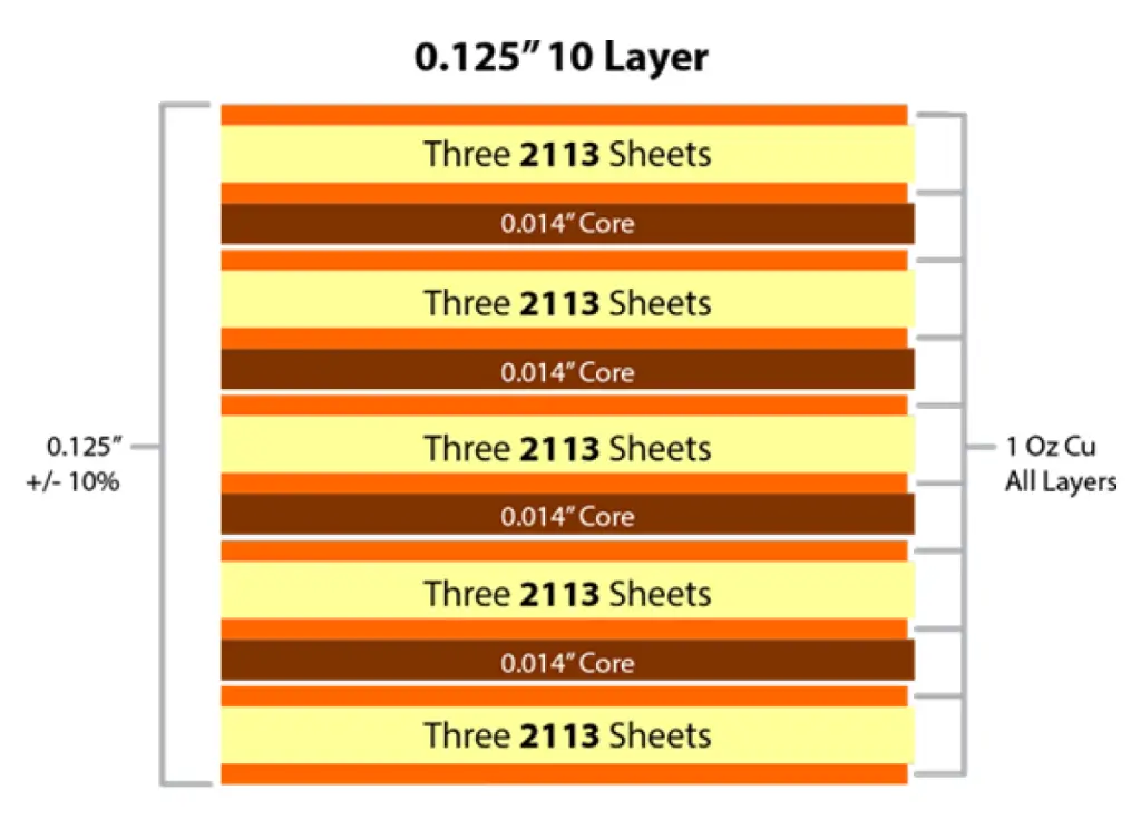
Multilayer PCB Lamination
Materials used in the lamination process include: inner layer core, sheets of “prepreg” (woven glass cloth with epoxy resin), and sheets of Cu foil. Tooling holes in each sheet of materials and core are used to align them as they are stacked up. For a 4 layers board, the bottom would be a sheet of foil, followed by a specific number of sheets of prepreg, the inner layer core. It is followed by more prepreg and finally the top sheet of foil. The stack of panels is built on a heavy metal plate and when it is completed a top plate is added creating a “book”. The book is then moved to a heated hydraulic press.
Pressure, heat, and a vacuum are applied over a 2 hours period forcing the resin from the prepreg to become elastic and flow across the core and foil surfaces. Once cured, the resin will join the glass sheets, core, and foil together into the multilayer PCB panel.
Multilayer PCB Wrap Plating
Wrap plating is where the drill hole is plated with copper as the plating extends from the hole drilled onto the board and onto the surface. This plating is made from copper; it extends from around the via structure and under the cap plating to move out from the surface.
There are different class specifications regarding the thickness of the electrolytic hole plating thickness. The IPC-6012 standard (and IPC-A-600 inspection standard) has a Class I, Class II, and Class III categories. Class I thickness specifications merely state that the thickness will be as agreed between the user and the supplier (AABUS). This is the least option used by most production facilities.
The Class II specification is where the wrap plating has to be continuous through the filled plated hole and it becomes extended on the PCBs surface. The thickness of the wrap plating can be no less than 5 μm [197 μin] for the via structures and through-holes. Also, the processing of the circuit board by means of planarization, sanding, and etching processes should not result in having insufficient wrap plating in place when these processes reduce the thickness of the copper material.
The Class III standard is similar to the Class II standard except that the minimum thickness of the wrap plating should not be below 12 μm [472 μin] for the through-holes, blind vias, and buried vias that are greater than 2 layers. Buried via cores must have a minimum thickness of 7 μm [276 μin] and both blind and buried microvias can have a minimum wrap thickness of 6 μm [236 μin].
There are many challenges associated with wrap plating of the PCB. Knee cracking is when expansion of the plating during thermal cycles of the PCB can result in the wrap plating developing stress cracks due to the temperature, number of PCB layers, and the CTE of the materials. Butt joint failures can also be a result caused by thermal cycles. Another challenge is meeting the minimum thickness standards during the planarization process that could vary the thickness of the wrap by ±0.3 mils.
Multilayer PCB Cost
If there is a downside to multilayer PCBs, it’s that they can be more expensive overall than their single—and double-layered counterparts. However, manufacturers who choose multilayer PCBs do so for their increased versatility and performance, which compensates for the increased cost.
More layers increase costs due to more materials and longer production times.
Specialty materials like high Tg FR-4 and polyimide are more expensive but necessary for high-performance boards.
Higher volumes can reduce the cost per unit, offering economies of scale.
Advanced techniques like HDI or the use of microvias add to the cost.
4 Layer PCB
With miniaturized electronic products becoming ubiquitous, the need for small circuit boards is on the rise. Multilayer circuit boards are therefore the order of the day. A 4-layer PCB stackup is becoming increasingly common. Let us look at the 4-Layered PCB in detail.
4 layers stackups are a popular jumping-off point for simple designs. As a cheap build with high design manufacturability, the four-layer design still exists alongside more intensive and expansive boards in today’s design world. Deciding upon a four-layer stackup begins by analyzing the number of components for placement and the routing needed.
4 Layer PCB Board Stackups
There’s at least a dozen ways to arrange layers in a four-layer stackup, but there are three types of four-layer stackups that are most common. These most common four-layer stackups recognize the fact that planes are being used, which is one of the main reasons to start using four-layer stackups. The three most common approaches to four-layer stackups are shown in the graphic below.
There can be 3 ways in which these can be stacked up
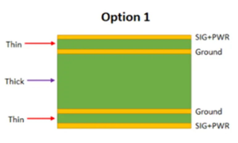
4 layer pcb stackup option 1
SIG+PWR/GND type stackups
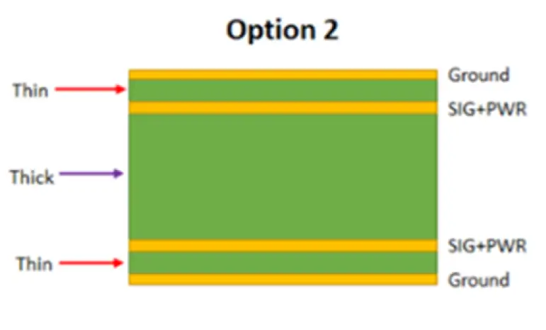
4 layer pcb stackup option 2
SIG/GND/PWR/SIG stackups
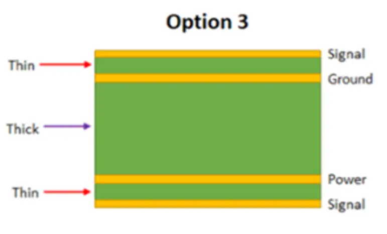
4 layer pcb stackup option 3
SIG/GND/SIG + PWR/GND stackups
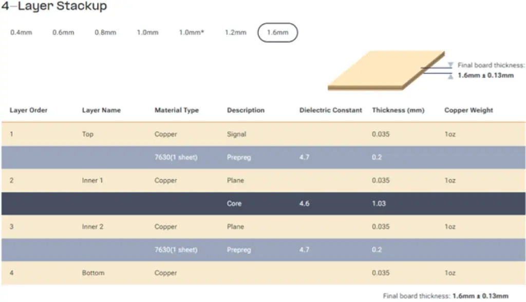
4 Layer PCB Stackup Thickness (Core and Prepreg Thickness)
4 Layer PCBs come with two types of Core & Prepreg thickness. The standard thickness is 1.6 mm (about 0.06 in) although 1.2 mm (about 0.05 in) is also commonly used.
We have already published article where you can check difference between PCB core and prepreg .
With a 1.6 mm (about 0.06 in) PCB, the core material is 1.2 mm (about 0.05 in) thick while the prepregs are 0.2 mm (about 0.01 in) each.
With 1.2 mm (about 0.05 in) thickness, there is a core material of 0.8mm (about 0.03 in), o.2 mm (about 0.01 in) of prepreg with coil and 0.2 mm (about 0.01 in) of prepreg with copper.
Four layer PCB stackup Example
PCB fabrication houses have standard stackups they will use for many builds, including four-layer PCBs. The four-layer stackup you find on a fabricator’s engineer could be standard thickness at 1.57 mm, although other common thickness values are available, such as 1 mm or 2 mm. If your design does not have strict material requirements, then the fabricator will use their standard stackup.
Typically, the standard stackups will be specified in a table such as that shown below. They will generally provide layer thickness and dielectric constant at a minimum, as well as two options for Tg values.
Multilayer PCB manufacturing process
There is no such thing as a standard printed circuit board. Each PCB has a unique function for a particular product. Therefore, producing a PCB is a complex, multi-stage process. This overview covers the most important steps when producing a multilayer PCB.
- PPE - Pre Production Engineering
- Material issue
- Inner layer
- Inner layer etch
- Inner layer AOI
- Lamination
- Drilling
- PTH - Plated Through Hole
- Panel plating
- Outer layer image
- Pattern plate
- Outer layer etch
- Outer layer AOI - Automated Optical Inspection
- Via hole plugging
- Soldermask
- Surface finish
- Profile
- ET - Electrical Test
- Final inspection
- Packaging
High Quality Multilayer PCB Vendor
The processes to manufacture multilayer printed circuit boards require specialized equipment and a significant commitment to operator training, not to mention the financial consideration. This explains why some fabricators have been slower to enter the multilayer manufacturing market than others. Benchuang Electronics can provide the expanded capabilities to support advanced printed circuit board designs with demanding requirements including laser drilled microvias, cavity boards, heavy copper up to 30 oz., via-in-pad, microwave & RF boards, up to 100 layers and others.
Get started with Multilayer PCB
- Blind vias, buried vias, Ultra HDI PCB
- High frequency low loss PCB material
- Low loss high speed PCB materials
- R-5775, R-5785, R-5795, TU-872 SLK , TU-872 SLK SP, TU 933+, I-Tera MT40, Astra MT77, Tachyon 100G material
- EM-888, EM-888(S), EM-888(K), EM-526, EM-528, EM-528K, IT-968, IT-968 SE, IT-988G, IT-988G SE material